


 The Right Approach: I Hear the Train A Comin'
 It’s Only Common Sense: OCCAM—the Time Is Now
 Marcy's Musings: The Growing Industry
Diagnosing Better Efficiencies for Solar Cells
December 14, 2015 | University of MarylandEstimated reading time: 2 minutes
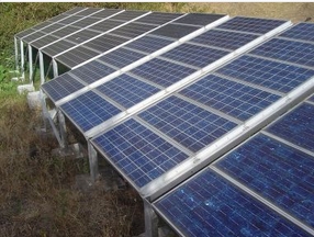
A new diagnostic imaging technique developed by a University of Maryland -led team of researchers promises to boost efficiencies of solar cells by making it possible to find and correct previously undetected ways that solar cells fall far short of theoretical efficiencies.
Theory indicates that current solar cell technologies should able to convert solar energy to electrical energy with at least 30 percent efficiency, but the actual efficiencies of current cells is only around 20 percent. Thus solar panels produce one third less power than the theoretical maximum of these devices.
“With the new imaging technique our team has developed, academic and industry researchers will be able to diagnose where solar cells lose efficiency and close the gap between theory and the actual efficiencies experienced by consumers who install solar panels on their homes and businesses,” said University of Maryland (UMD) Assistant Professor Marina Leite, in the UMD Institute for Research in Electronics and Applied Physics (IREAP) and the department of materials science & engineering in the
A. James Clark School of Engineering.
Solar cell efficiencies depend on the maximum achievable open-circuit voltage generated by the device under illumination. Open-circuit voltage determines how well any photovoltaic device operates, and researchers must be able to measure and image it in order to diagnose which processes are adding to or subtracting from cell efficiency.
The new, ambient temperature imaging technique presented by Leite and her team [Tennyson, et al] is a variation of illuminated Kelvin Probe Force Microscopy, which is a non-contact, non-destructive imaging technique used to determine the composition and electronic state of a surface. Traditionally, this technique uses a laser diode to scan the surface of a solid and measure the potential difference between the tip of the probe and the surface of that material. Tennyson, et al. takes this conventional imaging method further to demonstrate a “direct correlation between Kelvin Probe Force Microscopy measurements (light- minus dark-KPFM) and the open-circuit voltage of photovoltaic devices through the measurement of the quasi-Fermi level splitting”. This indirect measurement allows the UMD-led team to observe precisely [at nanoscale resolution] where the open-circuit voltage is changing.
The researchers say that previous imaging techniques for determining solar cell efficiencies had to be performed under vacuum at very cold temperatures (-333 Fahrenheit or 70 Kelvin). Their new technique fills an important gap in the literature surrounding solar cell efficiencies, providing a “straightforward, universal, and accurate method to measure the open-circuit voltage... with high spatial resolution,” they say.
The findings of Leite and her team are published in, and featured on the cover of, the December 9 issue of Advanced Energy Materials. “Nano-imaging of open-circuit voltage in photovoltaic devices,” Elizabeth Tennyson and Marina Leite*, IREAP and department of materials science & engineering, UMD; Joseph Garrett, IREAP and department of physics, UMD ; Jesse Frantz, Jason Myers, and Jasbinder S. Sanghera, U. S. Naval Research Laboratory; Robel Bekele, University Research Foundation; and Jeremy Munday, department of electrical and computer engineering and IREAP, UMD.
Share on:


Suggested Items
Taiyo Circuit Automation Installs New DP3500 into Fuba Printed Circuits, Tunisia
04/25/2024 | Taiyo Circuit AutomationTaiyo Circuit Automation is proud to be partnered with Fuba Printed Circuits, Tunisia part of the OneTech Group of companies, a leading printed circuit board manufacturer based out of Bizerte, Tunisia, on their first installation of Taiyo Circuit Automation DP3500 coater.
Determining the Value-add of Box Build
04/24/2024 | Nolan Johnson, I-Connect007At a strategic level, adding box-building services makes sense for customer loyalty. But is it really that simple? Jon Schmitz, who manages customer engagement at RiverSide Integrated Solutions, talk about about what it really takes to be successful in offering EMS and final assembly services under the same company banner.
Designer’s Notebook: What Designers Need to Know About Manufacturing, Part 2
04/24/2024 | Vern Solberg -- Column: Designer's NotebookThe printed circuit board (PCB) is the primary base element for providing the interconnect platform for mounting and electrically joining electronic components. When assessing PCB design complexity, first consider the component area and board area ratio. If the surface area for the component interface is restricted, it may justify adopting multilayer or multilayer sequential buildup (SBU) PCB fabrication to enable a more efficient sub-surface circuit interconnect.
Trackwise Awarded Prestigious King’s Award for Enterprise for Innovation
04/24/2024 | TrackwiseTrackwise Designs plc, the innovative manufacturer of specialist products using printed circuit technology, is delighted to be recognised with a prestigious King’s Award for Enterprise. Announced, Friday 21 April, Trackwise has been recognised for its excellence in Innovation for its length-unlimited, multilayer flexible printed circuits.
Three Industry Leaders Receive IPC President’s Award
04/17/2024 | IPCIn recognition of their leadership and significant contributions of time and talent to IPC and the electronics industry, three IPC volunteers were presented with the IPC President’s Award at IPC APEX EXPO in Anaheim, Calif., on April 9, 2024.