


 Dan’s Biz Bookshelf: ‘The Next RenAIssance: AI and the Expansion of Human Potential’
 The Chemical Connection: When the Industry Moves Faster Than the Standards
 Driving Innovation: Selecting the Right Laser Source


Heraeus and Intego Show a New Optical Inspection Method for Patterned Touch Sensors
August 4, 2016 | HeraeusEstimated reading time: 2 minutes
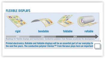
At this year Touch Taiwan from August 24-26, Heraeus launches a new touch panel process to pattern Clevios conductive polymer films by DFR (dry-film resist) photolithography. It enables high resolution patterns required for advanced touch sensor designs of flexible smartphones and tablets. Heraeus worked together with Intego on a new inspection method to visualize the invisible patterns of the Clevios sensor films. “With Intego, we found an excellent partner to offer a solution that enables our customers to accelerate the adoption of Clevios touch technology in mass production for flexible touch displays”, says Dr. Armin Sautter, Head of Technical Service Display at Heraeus. High resolution patterning of touch sensors is a prerequisite for advanced touch panels, especially for flexible and foldable touch displays. Dr. Thomas Wagner, CEO at Intego GmbH, emphazises “This is an important milestone, we are now able to offer a customized tool and a process for the inspection and quality control of the sensor patterning process for production environment.” A small scale demo tool will be shown at the Heraeus booth Taipei World Trade Center / Nangang Exhibition Hall 4F / N1029.
Patterned ITO films require additional optical compensation layers to hide the visible patterns in the touch panel. In contrast, both fine and wide Clevios patterns are already completely invisible after touch sensor production. No additional optical compensation layers are required in the touch panel process, offering customers cost benefits as well as process simplifications. Clevios conductive polymers are key materials for foldable touch sensors that will be used in the coming generations of flexible smartphones and tablets. Clevios coated films can be folded more than 300.000 times at a radius as low as 1 mm without degradation of the electro-optical properties.
About Intego GmbH
Intego GmbH, located in Erlangen, Germany, develops inspection systems for automated production lines used in a number of industries including glass/sapphire, solar, LED/OLED, electronics, automotive, plastics and medical technologies. (www.intego.de/en)
About Heraeus
Heraeus, the technology group headquartered in Hanau, Germany, is a leading international family-owned company formed in 1851. With expertise, a focus on innovations, operational excellence and an entrepreneurial leadership, we strive to continuously improve our business performance. We create high-quality solutions for our clients and strengthen their competitiveness in the long term by combining material expertise with technological know-how. Our ideas are focused on themes such as the environment, energy, health, mobility and industrial applications. Our portfolio ranges from components to coordinated material systems which are used in a wide variety of industries, including the steel, electronics, chemical, automotive and telecommunications industries. In the 2015 financial year, Heraeus generated revenues without precious metals of €1.9 bn and a total revenue of €12.9 bn. With approximately 12,500 employees worldwide in more than 100 subsidiaries in 38 countries, Heraeus holds a leading position in its global markets.
Share on:


Testimonial
"Your magazines are a great platform for people to exchange knowledge. Thank you for the work that you do."
Simon Khesin - Schmoll MaschinenSuggested Items
The Missing Connection: Wire Harness Quoting Joins the Digital Age
05/01/2026 | Joanne Harris, Tech-2marketingWalk the floor of a modern wire harness manufacturing facility, and the investment in technology is hard to miss. Automated wire cutting and stripping machines process thousands of cuts an hour with sub-millimeter precision. Computerized crimping presses deliver consistent, validated terminations that a hand tool never could. Laser wire markers, automated test benches, and vision-guided assembly stations represent hundreds of thousands of dollars of capital investment, all in service of building a better harness faster and more reliably than the competition.
EDADOC: Building the ‘Neural Hub’ for High-Compute Chips Within a Compact Space
04/28/2026 | ECIOEvery chip to the market must pass a stringent checkpoint before shipment known as ATE testing. Serving as the physical “neural hub” that connects test equipment worth millions of dollars with the device under test, the performance of the ATE test board directly determines the accuracy, efficiency, and final yield of chip testing. Amid the rapid rise of high-compute chips, what extreme challenges is this seemingly small circuit board facing? How is EDADOC addressing industry pain points through its one-stop “design + manufacturing” model?
The Chemical Connection: When the Industry Moves Faster Than the Standards
04/29/2026 | Don Ball -- Column: The Chemical ConnectionAs a supplier of wet processing equipment, we have rules and standards we must adhere to, including both regional and national electrical codes and safety and environmental regulations, as well as myriad other standards to make the equipment safe to use. Things are a little different when it comes to rules and standards for manufacturing PCBs, though, because technical advances and requirements change so quickly that standards can’t keep up.
Driving Innovation: Selecting the Right Laser Source
04/28/2026 | Simon Khesin -- Column: Driving InnovationWhen I first joined Schmoll Maschinen, I brought experience from almost every PCB process, except for laser. As I immersed myself in laser processing, I realized why it can seem so daunting to a newcomer. The complexity arises from three intersecting factors: A vast variety of laser sources: CO2, UV-nano, green-pico, UV-pico, IR-pico, and others; a diverse range of applications: Drilling, cutting, ablation, and more; and an extensive list of materials: These have vastly different absorption rates. Choosing the right machine or laser source is rarely trivial. Even for experienced engineers, answering "Which source is best?" requires examining the business's specific goals.
Market Insights with Pluritec's Maurizio Bonati
04/23/2026 | Real Time with... APEX EXPONolan Johnson interviews Maurizio Bonati, VP of Sales at Pluritec, at APEX EXPO 2026. Bonati details Pluritec's three product divisions, covering a broad spectrum of PCB manufacturing. He discusses the current robust electronics market, driven by AI applications in Asia and technological investments in North America, while noting slower demand in Europe. The interview highlights key sectors like data centers, AI, and medical that benefit from advanced electronics.