


 Smart Automation: The Journey of a Component Through an SMT Factory
 Powering the Future: Why Thermal Management Defines the Future of Electronics
 Standard of Excellence: Engineering Is the New Sales—How Technical Collaboration Wins Business


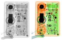
2D X-ray Inspection With Materials and Thickness Identification
June 7, 2017 | Paul D. Scott, Ph.D., IBEX Innovations, and Evstatin Krastev, Ph.D., P.E., Nordson DageEstimated reading time: 7 minutes
ABSTRACT
X-ray inspection systems are key tools for quality control, yield enhancement, and failure analysis of PCBs and semiconductor devices. In many cases, these capable tools provide the only non-destructive techniques for inspection of electronic components. There have been significant improvements in the X-ray inspection capabilities (both 2D and 3D) in the last several years. In this paper we report a new development that permits material and thickness information to be obtained via 2D X-ray inspection.
While absorption contrast X-ray imaging is a very powerful inspection technique, it does not exploit all of the information present within the X-ray beam transmitted through a sample. A new technology has been recently developed that, instead of simply measuring the total absorption of the X-ray beam, also enables changes in the beam energy to be resolved. This allows the effects of thickness and density to be decoupled, enabling both to be determined. This quantitative composition and thickness information can then be used to provide new levels of insight in PCB and semiconductor inspection, potentially leading the way to a new generation of X-ray inspection technology.
It is quite straightforward to accommodate this technology in an existing 2D X-ray (2DX) inspection system. Advanced software algorithms need to be incorporated and an intuitive user interface is provided.
We present an overview of this new technology and give examples of other industries where this technology is being adopted, as well as example applications for the PCB and semiconductor industries.
INTRODUCTION
The need to inspect electronic components and assemblies non-destructively is the main driver behind the development and advancement of the X-ray inspection technology for the electronics industry. In many cases, X-Ray inspection (2D and 3D) provides the only non-destructive techniques to inspect optically hidden components and solder joints such as BGA, POP, QFN, flip chips, through holes, TSVs, microbumps, copper pillars, etc.
All X-ray inspection systems (2D and 3D) rely on absorption contrast imaging, where the contrast is generated by the stopping power of the sample. As such, higher density and/or thicker regions of a sample produce darker regions in a grey-scale image. X-ray inspection systems use this method to image features such as wire bonds and ball grid arrays down to a feature recognition size of 100 nm (0.1 μm).
While contrast imaging is a very powerful and widely used technique, there is significantly more information present within the X-ray beam, which, until now, has not been exploited in electronics inspection. Instead of simply measuring the total absorption of the X-ray beam, a physical structure known as a multi absorption plate (MAP) can be placed in the beam path. This, coupled with machine learning algorithms, enables material type and thickness information to be acquired alongside the standard grey-scale image.
Quantitative composition and thickness information can then be used to provide more detailed diagnostics in PCB and semiconductor inspection. Applications include, but are not limited to, analysis of solder types, track thickness measurements, and conformance to quality standards.
An overview of the theory behind the operation of the MAP is given below, as well as some simple examples showing the benefits of using the MAP technology to add additional capabilities to 2D X-Ray inspection. MAP technology also has applications in the security, medical and food processing industries. Nordson Dage has partnered with IBEX to bring the benefits of this technology to the electronics inspection, including inspection of PCBs and semiconductor devices. A range of examples is presented and the authors aim to start active discussions that would generate new needs and ideas for use of the technology for non-destructive inspection of electronics systems and components.
BASIC PRINCIPLES OF THE MAP TECHNOLOGY
X-ray Interaction with a Sample
X-rays are generated using a tungsten target which produces a continuous spectrum, known as Bremβtrahlung radiation, as well as characteristic peaks at specific energies.
Adding a sample such as a printed circuit board into the beam attenuates the X-ray spectrum in the following way:
I(E) = I0(E)exp(-µ(E)t) (1)
where I0(E) and I(E) are the intensities of the X-ray spectra before and after the sample, respectively; µ(E) is the material-dependent linear attenuation coefficient; and t is the thickness of the sample.
If I0(E) and I(E) can be determined, it is possible to extract the parameter µ(E) which relates to the material type and the material thickness.
A standard CMOS detector integrates the total energy deposited into each pixel over the user-selected integration time. As such, the detector is able to measure total energy deposited per pixel but not the actual energy spectrum. This means that it is not possible to decouple the material and thickness terms in equation (1), meaning that thin, high density materials are indistinguishable from thick, low density materials in a single 2D projection.
The Multi Absorption Plate (MAP) acts like a complex color filter for the X-rays by imposing a repeating modulation to the X-ray beam over a few neighboring pixels. This modulation results in a variation in the energy distribution of the X-ray beam incident on the neighboring pixels in a way that enables unique materials information to be obtained.
Extracting Materials Information—Simple Examples
Figure 1 shows the word IBEX constructed using a series of copper tiles with a background made up of foils of silver. The thicknesses of the foils have been selected in order to randomize the grey-scale intensity transmitted by the tiles and hence obscure the word IBEX in a standard X-ray image. Analyzing the image with a MAP in place recovers the materials information. The intensities of the coloring in the bottom image of Figure 1 reflect the relative thicknesses of the tiles.
Figure 1: Optical image showing the word IBEX created as a mosaic of random thicknesses of silver and copper foils (top); X-ray transmission image showing that it is not possible to distinguish between the foils using absorption contrast alone (middle); materials contrast image showing that the missing information can be recovered using the MAP (bottom).
This materials information can be displayed to the user in terms of a basic mask identifying the materials, as an overlay of material identification on the absorption contrast image, or in the case of automated quality inspection systems as a pass/fail criterion.
Page 1 of 2
Share on:


Testimonial
"Our marketing partnership with I-Connect007 is already delivering. Just a day after our press release went live, we received a direct inquiry about our updated products!"
Rachael Temple - AlltematedSuggested Items
ACCM Unveils Negative and Near-zero CTE Materials for Large-Format AI Chips
04/21/2026 | Advanced Chip and Circuit MaterialsAdvanced Chip and Circuit Materials, Inc. (ACCM) has launched two new materials: Celeritas HM50, with a negative coefficient of thermal expansion (CTE) of -8 ppm/°C to offset the positive CTE and expansion of copper with temperature on circuit boards, and Celeritas HM001, with near-zero CTE and the low-loss performance needed for high-speed signal layers to 224 Gb/s and faster in artificial intelligence (AI) circuits.
SMTA Ultra HDI Symposium, Day 2: Fragile Supply Chains, Fierce Innovation
04/14/2026 | Marcy LaRont, I-Connect007The Arizona weather yielded another beautiful day as we gathered for the second day of SMTA’s annual UHDI symposium. After the first full day discussing the role of AI in business and the how-tos of implementation, Avondale Mayor Mike Pineda kicked off day two, proud to showcase his city and to declare its important place in the continued development of the West Valley, an increasingly important area for tech and manufacturing.
KYZEN Focuses on Aqueous and Stencil Cleaning Solutions at SMTA Monterrey Expo and Tech Forum
04/10/2026 | KYZEN'KYZEN, the global leader in innovative environmentally friendly cleaning chemistries, will exhibit at the SMTA Monterrey Expo & Tech Forum.
Solder Paste Innovations for Enhanced Reliability from MacDermid Alpha Electronics Solutions
04/10/2026 | Real Time with... APEX EXPOJason Fullerton of MacDermid Alpha Electronics Solutions discusses innovative alloys like Innolot MXE, low-temperature solder options, and polymer reinforcement strategies. Learn how these solutions address the growing demands of high-performance computing and larger component assemblies, ensuring optimal performance and cost-effectiveness.
Frank Sommer Discusses Selective Soldering Innovations for EVs
04/10/2026 | Real Time with... APEX EXPODan Beaulieu sits down with Frank Sommer, a selective soldering expert from Nordson Electronics Solutions, to discuss the resurgence of selective soldering driven by electric vehicle manufacturing, and the need for robust through-hole component integration. He also introduces Nordson's innovative SELECT Synchro selective soldering machine, designed for enhanced throughput and flexibility.