


 Knocking Down the Bone Pile: Revamp Your Components with BGA Reballing
 Global Sourcing Spotlight: Balancing Speed and Flexibility Without Sacrificing Control
 SMT Perspectives & Prospects: Artificial Intelligence Part 6: Data Module 1


Rework and Reball Challenges for Wafer Level Packages
October 16, 2017 | Lauren Cummings and Priyanka Dobriyal, Ph.D., Intel Corp.Estimated reading time: 6 minutes
There is a growing consumer demand for smart wearable products, including watches, fitness bands, eyewear, and headphones. Barriers to the market still exist, as many consumers are concerned with style, battery life, functionality, and cost. The mature smartphone market faces similar challenges, with consumers desiring thinner phones with longer battery life and increased sensor functionality. High-density and stacked PCB designs, system in package (SiP) assemblies, and small form factor packages have all emerged as solutions for sleeker styles and improved functionality. In particular, WLPs are gaining popularity for their low cost, small footprint, and thin profile. The newest smartphone models contain an average of 5-7 WLPs, with many WLPs used as RF transceivers, power management units, audio amplifiers, and BlueTooth and GPS modules.
Figure 1: Cross-section schematics of (a) a traditional fan-in wafer level package, and (b) a newer fan-out wafer level package.
Unlike traditional packages, WLPs are packaged and bumped first, then diced. Passivation and dielectric layers are added to the die frontside, followed by metallic redistribution layers. A second dielectric layer is deposited, then the underbump metallization and solder balls are attached. Lastly, the packages are singulated from the wafer. Figure 1 illustrates the two different categories of WLPs: the traditional a) fan-in WLP, and the newer b) fan-out WLP. The dielectric is exposed on the edges and frontside of fan-in WLPs, while the silicon backside is often covered with a protection tape. As the name suggests, fan-out WLPs “fan out” interconnects from the smaller silicon die to the larger package dimensions. The fan-out design allows for ball pitch customization, higher I/O density, and easy integration with SiPs and other multidie packages. The board-level reliability is also improved by protecting the silicon die with an epoxy mold compound.
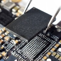
Though WLPs offer considerable advantages, they also pose challenges for failure analysis—particularly when reball and component-level testing are required. Figure 2 illustrates the typical FA process flow for a failing system, such as a mobile phone, tablet, or wearable device.
Figure 2: Diagram showing the typical process flow for system-level failure analysis
Fault isolation is performed first to identify the failing component, then nondestructive FA is used to inspect for failures at both the board- and package-level. If the failure is subtle or cannot be found non-destructively, the package must be reworked and reballed before proceeding with socketed component-level testing and further FA. Due to their small form factor and fragility, WLPs can prove particularly difficult for the rework and reball process steps. The present work provides an overview of the FA process flow, emphasizing component rework and reball methodologies. The challenges of a specific WLP case study are discussed, and rework and reball improvements are implemented to minimize thermally- or mechanically-induced artifacts.
Fault isolation is an important first step in the system-level FA process. By isolating the failure to a specific package or interconnect, an optimal FA approach can be assessed and throughput time can be greatly reduced. Several fault isolation techniques can be used to measure for opens and shorts, including hand probing, time domain reflectometry and the newer electro optic terahertz pulse reflectometry. High-resistance shorts can also be detected by powering the board and measuring the localized temperature increase using infrared thermal imaging techniques.
After the failing component has been isolated, nondestructive FA is performed to inspect for gross board- or package-level failures. OM can be used to inspect for external board or package defects, such as foreign materials or superficial die and overmold cracks. Since WLPs have exposed dielectric layers (and since fan-in WLPs have exposed bulk Si), it is especially important to perform a first pass inspection for external chips or cracks. It is recommended that optical inspection be performed again after rework and reball, to confirm that no artifacts were introduced.
CSAM, a popular non-destructive technique, can be utilized to detect internal defects or to evaluate the extent of external damage. CSAM uses an ultrasound transducer to raster-scan the package backside. At material interfaces, an acoustic pulse is reflected to the transducer and recorded as signal amplitude. Air-solid interfaces occur at the locations of cracks, voids, or delamination, and return high-intensity reflections. CSAM is thus a valuable metrology for identifying gross internal package defects that cannot be detected with simple optical inspection. CSAM can also be used to screen for rework and reball artifacts, particularly thermally- induced delamination.
2D X-ray is another common technique that provides an effective “quick pass” inspection for board-level solder defects, such as voids and bridging. By optimizing the sample tilt and rotation angles, subtler non-wet open and noncontact open defects can also be detected. However, 2D X-ray is not capable of detecting submicron defects, such as board-level solder or via cracks.
Recently, more advanced imaging metrologies have emerged as powerful non-destructive FA techniques. In particular, 3D X-ray computed tomography has proven effective at detecting both board-level and package-level sub-micron defects. Multiple 2D X-ray images are collected as the sample is rotated at fixed angle increments. The 2D X-ray images are then superimposed to generate a three-dimensional volume. The superimposed image can be manipulated to display virtual “slices” of the sample, allowing for inspection of the solder joints, via barrels, and traces.
If board-level or gross package-level failures are not detected using non-destructive techniques, the package must be sent for socketed component-level testing and further FA. Standard test sockets use a spring-loaded floating base that is guided by the solder balls instead of the package edge. Reball is thus required to align the package and enable good electrical contact with each pin. It is very important to preserve the defect signature prior to testing; accordingly, precautions must be taken to improve the reball yield and reduce thermal and mechanical artifacts.
Page 1 of 2
Share on:


Testimonial
"We’re proud to call I-Connect007 a trusted partner. Their innovative approach and industry insight made our podcast collaboration a success by connecting us with the right audience and delivering real results."
Julia McCaffrey - NCAB GroupSuggested Items
Rehm Wins Mexico Technology Award for CondensoXLine with Formic Acid
10/17/2025 | Rehm Thermal SystemsModern electronics manufacturing requires technologies with high reliability. By using formic acid in convection, condensation, and contact soldering, Rehm Thermal Systems’ equipment ensures reliable, void-free solder joints — even when using flux-free solder pastes.
Indium Experts to Deliver Technical Presentations at SMTA International
10/14/2025 | Indium CorporationAs one of the leading materials providers to the power electronics assembly industry, Indium Corporation experts will share their technical insight on a wide range of innovative solder solutions at SMTA International (SMTAI), to be held October 19-23 in Rosemont, Illinois.
Knocking Down the Bone Pile: Revamp Your Components with BGA Reballing
10/14/2025 | Nash Bell -- Column: Knocking Down the Bone PileBall grid array (BGA) components evolved from pin grid array (PGA) devices, carrying over many of the same electrical benefits while introducing a more compact and efficient interconnect format. Instead of discrete leads, BGAs rely on solder balls on the underside of the package to connect to the PCB. In some advanced designs, solder balls are on both the PCB and the BGA package. In stacked configurations, such as package-on-package (PoP), these solder balls also interconnect multiple packages, enabling higher functionality in a smaller footprint.
Indium to Showcase High-Reliability Solder and Flux-Cored Wire Solutions at SMTA International
10/09/2025 | Indium CorporationAs one of the leading materials providers in the electronics industry, Indium Corporation® will feature its innovative, high-reliability solder and flux-cored wire products at SMTA International (SMTAI), to be held October 19-23 in Rosemont, Illinois.
‘Create your Connections’ – Rehm at productronica 2025 in Munich
10/08/2025 | Rehm Thermal SystemsThe electronics industry is undergoing dynamic transformation: smart production lines, sustainability, artificial intelligence, and sensor technologies dominate current discussions.