


 The Chemical Connection: Reducing Etch System Water Usage, Part 2
 It’s Only Common Sense: Nice Guys Really Can Finish First
 The Right Approach: I Hear the Train A Comin'
Eco-friendly Waterborne Semiconductor Inks Using Surfactant
November 27, 2017 | DGISTEstimated reading time: 1 minute
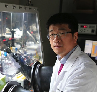
A team of researchers at DGIST, led by Professor Dae Sung Chung of Energy Science and Engineering has developed a technology to produce environmentally friendly water-borne semiconductor inks using surfactant, which is additives that mix substances of different properties and a component of soap.
Polymer semiconductors are carbon compounds showing the electrical properties of semiconductors. It has been highlighted as a next-generation material of wearable smart devices, etc. not only because they are flexible and light in weight, but also they can be processed in a wide area a low cost through the solution process. However, there is an issue that it causes significant environmental pollution as toxic organic solvents are used in the process.
Despite the limitations, the research team has developed a semiconductor surface control technique using surfactants for environmentally friendly semiconductor manufacturing processes that do not use toxic organic solvents and has produced water-borne semiconductor inks.
In the study, the newly developed waterborne semiconductor ink of the research team has small colloidal particles and less surfactant micelles compared to the waterborne semiconductor inks in the previous studies. As a result, it has a relatively flat surface than the conventional waterborne semiconductor inks. The black and white image in the below figure shows the comparison of the surface of the thin film made with the waterborne semiconductor ink developed in this study and conventional one.
According to the research team, the technique is expected to be applied in various electronic devices such as P-type and N-type transistors as well as PN diodes, complementary inverters, photodiodes as high-quality thin films.
Professor Chung stressed the significance of the study by stating "This research has fundamentally solved the environmental pollution problem generated during the production of organic semiconductor, which is spotlighted as the core material of wearable electronic devices. We have developed a source technology that can disperse various semiconductor materials into water through the simple chemical modification. We expect that it can be used in various optoelectronic devices ranging from transistors to solar cell, composite circuit, and image sensor.”
Share on:


Suggested Items
Altair Acquires Research in Flight, Forging a New Path for Aerodynamic Analysis
05/03/2024 | AltairAltair a global leader in computational intelligence, announced it has acquired Research in Flight, maker of FlightStream®, which provides computational fluid dynamics (CFD) software with a large footprint in the aerospace and defense sector and a growing presence in marine, energy, turbomachinery, and automotive applications.
Intel Takes Next Step Toward Building Scalable Silicon-Based Quantum Processors
05/02/2024 | BUSINESS WIRENature published an Intel research paper, “Probing single electrons across 300-mm spin qubit wafers,” demonstrating state-of-the-art uniformity, fidelity and measurement statistics of spin qubits.
Argonne, Toyota Collaborate on Cutting-Edge Battery Recycling Process
05/01/2024 | BUSINESS WIREThe U.S. Department of Energy’s (DOE) Argonne National Laboratory has recently launched a collaboration with Toyota Motor North America that could reduce the nation’s reliance on foreign sources of battery materials.
Chinese Smartphone Market Maintains its Recovery Momentum at 6.5% Growth in 1Q24,
04/26/2024 | IDCAccording to preliminary data from the International Data Corporation (IDC) Worldwide Quarterly Mobile Phone Tracker, China smartphone shipments grew 6.5% year over year (YoY) to 69.3 million units in 1Q24.
Boeing Opens Research & Technology Center in Japan
04/23/2024 | BoeingBoeing today opened a Boeing Research & Technology (BR&T) Center in Japan that will focus on innovation to enable the commercial aviation industry meet its goal of net zero carbon emissions by 2050.