


 It’s Only Common Sense: Nice Guys Really Can Finish First
 The Right Approach: I Hear the Train A Comin'
 Marcy's Musings: The Growing Industry
Understanding the Generation of Light-Induced Electrical Current in Atomically Thin Nanomaterials
May 23, 2018 | Brookhaven National LaboratoryEstimated reading time: 5 minutes
Scientists at the Center for Functional Nanomaterials (CFN)—a U.S. Department of Energy (DOE) Office of Science User Facility at Brookhaven National Laboratory—have used an optoelectronic imaging technique to study the electronic behavior of atomically thin nanomaterials exposed to light.
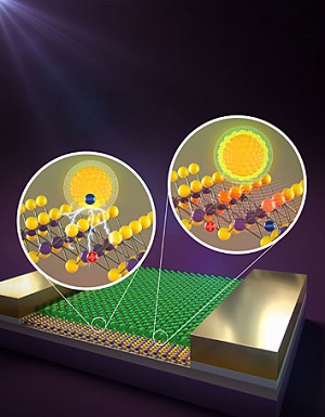
Image caption: A field-effect transistor (the device) containing molybdenum disulfide (stick and balls) doped with core-only quantum dots undergoing charge transfer (left zoom; charge transfer is shown as sparks) and core/shell quantum dots undergoing energy transfer (right zoom; energy transfer is shown as a wave moving from the quantum dots to molybdenum disulfide).
Combined with nanoscale optical imaging, this scanning photocurrent microscopy technique provides a powerful tool for understanding the processes affecting the generation of electrical current (photocurrent) in these materials. Such an understanding is key to improving the performance of solar cells, optical sensors, light-emitting diodes (LEDs), and other optoelectronics—electronic devices that rely on light-matter interactions to convert light into electrical signals or vice versa.
“Anyone who wants to know how light-induced electrical current is distributed across a semiconductor will benefit from this capability,” said CFN materials scientist Mircea Cotlet, co-corresponding author on the May 17 Advanced Functional Materials paper describing the work.
Generating an electrical current
When hit with light, semiconductors (materials that have an electrical resistance in between that of metals and insulators) generate an electric current. Semiconductors that consist of one layer or a few layers of atoms—for example, graphene, which has a single layer of carbon atoms—are of particular interest for next-generation optoelectronics because of their sensitivity to light, which can controllably alter their electrical conductivity and mechanical flexibility. However, the amount of light that atomically thin semiconductors can absorb is limited, thus limiting the materials’ response to light.
To enhance the light-harvesting properties of these two-dimensional (2D) materials, scientists add tiny (10–50 atoms in diameter) semiconducting particles called quantum dots in the layer(s). The resulting “hybrid” nanomaterials not only absorb more light but also have interactions occurring at the interface where the two components meet. Depending on their size and composition, the light-excited quantum dots will transfer either charge or energy to the 2D material. Knowing how these two processes influence the photocurrent response of the hybrid material under different optical and electrical conditions—such as the intensity of the incoming light and applied voltage—is important to designing optoelectronic devices with properties tailored for particular applications.
“Photodetectors sense an extremely low level of light and convert that light into an electrical signal,” explained Cotlet. “On the other hand, photovoltaic devices such as solar cells are made to absorb as much light as possible to produce an electrical current. In order to design a device that operates for photodetection or photovoltaic applications, we need to know which of the two processes—charge or energy transfer—is beneficial.”
(Left to right) Mingxing Li, Mircea Cotlet, Chang-Yong Nam, and Percy Zahl at the new scanning photocurrent microscopy facility at Brookhaven Lab's Center for Functional Nanomaterials.
Page 1 of 2
Share on:


Suggested Items
Indium Corporation Expert to Present on Pb-Free Solder for Die-Attach in Discrete Power Applications
04/30/2024 | Indium CorporationIndium Corporation Product Manager – Semiconductor Dean Payne will present at the Advanced Packaging for Power Electronics conference, hosted by IMAPS, held May 8-9 in Woburn, Massachusetts, USA.
Real Time with... IPC APEX EXPO 2024: Adhesive Materials and Equipment Update with Dymax
05/01/2024 | Real Time with...IPC APEX EXPOVirginia Hogan, global business development manager at Dymax, discusses adhesive materials, dispensing and curing equipment, a new, high-reliability conformal coating, and various materials and dispensing methods.
Real Time with... IPC APEX EXPO 2024: Sustainability in the Industry
04/26/2024 | Real Time with...IPC APEX EXPOGuest Editor Henry Crandall and Chris Nash of Indium Corporation discuss the company's 90th anniversary and its focus on sustainability. They focus on the benefits of sustainable materials, their compatibility, and value propositions. The conversation also highlights how Durafuse LT technology's role in reducing reflow temperatures is leading to significant cost and energy savings. Nash also touches on downstream sustainability efforts such as using recycled materials for packaging.
SMC Korea 2024 to Highlight Semiconductor Materials Trends and Innovations on Industry’s Path to $1 Trillion
04/24/2024 | SEMIWith Korea a major consumer of semiconductor materials and advanced materials a key driver of innovation on the industry’s path to $1 trillion, industry leaders and experts will gather at SMC (Strategic Materials Conference) Korea 2024 on May 29 at the Suwon Convention Center in Gyeonggi-do, South Korea to provide insights into the latest materials developments and trends. Registration is open.
Groundbreaking Ceremony Marks the Beginning of a New Era for Newccess Industrial; The Construction of the MINGXIN Building
04/12/2024 | Newccess IndustrialOn a clear and sunny day in March, the groundbreaking ceremony for the MINGXIN Building took place in Shenzhen, China. This moment marked the official commencement of construction for a project that will reshape the semiconductor materials industry.