


 The Right Approach: I Hear the Train A Comin'
 It’s Only Common Sense: OCCAM—the Time Is Now
 Marcy's Musings: The Growing Industry
Insulator-metal Transition at the Nanoscale
May 25, 2018 | ICFOEstimated reading time: 2 minutes
An international team of researchers is able to probe the insulator-conductor phase transition of materials at the nanoscale resolution. Controlling the flow of electrons within circuits is how electronic devices work. This is achieved through the appropriate choice of materials. Metals allow electrons to flow freely and insulators prevent conduction. In general, the electrical properties of a material are determined when the material is fabricated and cannot be changed afterwards without changing the material. However, there are materials that can exhibit metal or insulator behaviour depending on their temperature. Being able switch their properties, these materials could lead to a new generation of electronic devices.
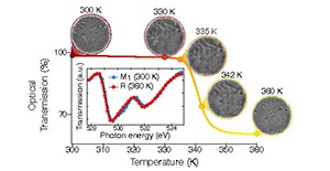
Vanadium Dioxide (VO2) is one such material. It can switch from an insulating phase to a metallic phase just above room temperature, a feature exploited already for sensors. However, the reason why the properties of this material change so dramatically has been a matter of scientific debate for over 50 years.
One of the challenges in understanding why and how this switch occurs is due to a process called phase separation. The insulator-metal phase transition is similar to the ice to liquid transition in water. When ice melts, both liquid and solid water can coexist in separate regions. Similarly, in VO2, insulating and metallic regions of the material can be coexisting at the same time during the transition. But unlike water, where the different regions are often large enough to see with the naked eye, in VO2 this separation occurs on the nanoscale and it is thus challenging to observe. As a result, it has been hard to know if the true properties of each phase, or the mixture of both phases, are being measured.
X-rays are a key tool for understanding the properties of materials, but it has been hard to use them to probe materials on the nanoscale because it is hard to build lenses for microscopes that can detect them. However, in a recent study published in Nano Letters, a team of researchers from ICFO and ALBA in Barcelona, the Technisch Universitat and Max-Born Institute in Berlin, and Vanderbilt University in Tennessee, has finally been able to probe the phase transitions that occur in thin films of Vanadium Dioxide (VO2) using resonant soft X-ray holography. This technique is capable of imaging the electronic and structural changes in this material with an unprecedented resolution at the nanoscale without the need of a len. By looking at the material with 50 nm resolution, the scientists were able to observe that defects in the material played an important role in initiating the phase transition from the insulator to the metal. However, more importantly, the authors also observed a third intermediate state formed during the phase transformation. Whilst some regions transformed directly from the insulating to metallic phase, others transformed into a second different insulating state before becoming metallic at higher temperatures with the exact pathway taken depending on the defects present in the material. The coexistences of three phases has radically changed the views of previous studies that assumed the presence of only two states during the transition. Even more, the study presents new ways in which the transition could be controlled.
In addition to the results obtained on the phase transition in VO2, the work also highlights the possibilities that X-ray holography can bring for studying materials on the nanoscale. The technique is the only method that can image real-time nanoscale dynamics and is now being used to study the properties of other intriguing materials such as high temperature superconductors.
Share on:


Suggested Items
Real Time with... IPC APEX EXPO 2024: Sustainability in the Industry
04/26/2024 | Real Time with...IPC APEX EXPOGuest Editor Henry Crandall and Chris Nash of Indium Corporation discuss the company's 90th anniversary and its focus on sustainability. They focus on the benefits of sustainable materials, their compatibility, and value propositions. The conversation also highlights how Durafuse LT technology's role in reducing reflow temperatures is leading to significant cost and energy savings. Nash also touches on downstream sustainability efforts such as using recycled materials for packaging.
SMC Korea 2024 to Highlight Semiconductor Materials Trends and Innovations on Industry’s Path to $1 Trillion
04/24/2024 | SEMIWith Korea a major consumer of semiconductor materials and advanced materials a key driver of innovation on the industry’s path to $1 trillion, industry leaders and experts will gather at SMC (Strategic Materials Conference) Korea 2024 on May 29 at the Suwon Convention Center in Gyeonggi-do, South Korea to provide insights into the latest materials developments and trends. Registration is open.
Groundbreaking Ceremony Marks the Beginning of a New Era for Newccess Industrial; The Construction of the MINGXIN Building
04/12/2024 | Newccess IndustrialOn a clear and sunny day in March, the groundbreaking ceremony for the MINGXIN Building took place in Shenzhen, China. This moment marked the official commencement of construction for a project that will reshape the semiconductor materials industry.
The Need for a Holistic Global Sustainability Standard
04/10/2024 | Michael Ford, Aegis SoftwareNo one can deny that the resources of our fragile planet are finite. The environment seems like a third party, subject to constant degradation. We’re acutely aware of the effects of pollution on our climate, and despite our “throw-away” culture, recycling and recovery of materials has remained relatively expensive, even as we use more energy just to survive.
iNEMI Publishes Four Roadmap Topics
04/04/2024 | iNEMIThe International Electronics Manufacturing Initiative (iNEMI) announces the availability of the first roadmap topics in the new iNEMI Roadmap format. Printed circuit boards, sustainable electronics, smart manufacturing, and mmWave materials and test are now available online.