


 It’s Only Common Sense: Nice Guys Really Can Finish First
 The Right Approach: I Hear the Train A Comin'
 Marcy's Musings: The Growing Industry
Light, Finely Sliced
July 16, 2018 | A*STAREstimated reading time: 2 minutes
A plan to incorporate a third bent waveguide into a silicon-based light splitter led A*STAR researchers to develop a device capable of a 30-fold improvement in splitting efficiency. The novel on-chip light splitter marks a major breakthrough in improving high-performance data transmission systems, as well as applications in quantum computing.
The manipulation of light in micro-scale devices is a fundamental pillar of high-speed optical circuits underpinning communications and next-generation technologies like quantum computing. Light is fast and low-power, and can be encoded to transmit data in a variety of ways. As Thomas Ang from the A*STAR Institute of High Performance Computing (IHPC) explains, for these manipulations to be reliable and efficient, the light needs to be as ‘pure’ as possible — not just tightly confined around a specific wavelength, but also of a uniform polarization.
“Light consists of a mixture of two polarization components,” Ang says. “Polarization beam splitters are used to separate a mixed-polarization beam into two channels for each polarization.”
When the splitting is imperfect, the two channels can contain small proportions of the opposite polarization, an effect known as crosstalk.
“Polarization beam splitters with low crosstalk are very important for high signal fidelity in high-speed optical interconnect applications,” says Jun Rong Ong, Ang’s partner in the study. “Current technology is limited to a crosstalk level, called the extinction ratio, of around 25 decibels, which is high enough to affect high-speed data transmission.”
The field of polarization beam splitters (PBSs) is well-developed, and there have been many attempts to break this 25 decibel limit in silicon-based devices as the industry standard for fabrication. Ang, Ong and their colleagues brainstormed ways to challenge this limit, and came up with the idea of adding a third waveguide — essentially a channel or path to route light on a chip — when the status quo dictated no more than two.
“We were interested in waveguides for bending and routing light, and conceptualized our new design after brainstorming within our team,” says Ang. “We tested our hypothesis using computer simulations and were thrilled to find that the device outperformed some of the best-in-class published results.”
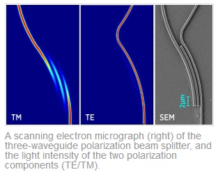
Working with collaborators at the Singapore University of Technology and Design, the team then fabricated the three-waveguide device (see image) and confirmed its vastly improved extinction ratio of 40 decibel, representing a further 30-fold reduction in polarization crosstalk.
“We also expect that the device can be improved further by optimizing its design,” says Ong.
Share on:


Suggested Items
IPC's Vision for Empowering PCB Design Engineers
04/30/2024 | Robert Erickson, IPCAs architects of innovation, printed circuit board designers are tasked with translating increasingly complex concepts into tangible designs that power our modern world. IPC provides the necessary community, standards framework, and education to prepare these pioneers as they explore the boundaries of what’s possible, equipping engineers with the knowledge, skills, and resources required to thrive in an increasingly dynamic field.
iNEMI Packaging Tech Topic Series: Role of EDA in Advanced Semiconductor Packaging
04/26/2024 | iNEMIAdvanced semiconductor packaging with heterogenous integration has made on-package integration of multiple chips a crucial part of finding alternatives to transistor scaling. Historically, EDA tools for front-end and back-end design have evolved separately; however, design complexity and the increased number of die-to-die or die-to-substrate interconnections has led to the need for EDA tools that can support integration of overall design planning, implementation, and system analysis in a single cockpit.
Cadence, TSMC Collaborate on Wide-Ranging Innovations to Transform System and Semiconductor Design
04/25/2024 | Cadence Design SystemsCadence Design Systems, Inc. and TSMC have extended their longstanding collaboration by announcing a broad range of innovative technology advancements to accelerate design, including developments ranging from 3D-IC and advanced process nodes to design IP and photonics.
Ansys, TSMC Enable a Multiphysics Platform for Optics and Photonics, Addressing Needs of AI, HPC Silicon Systems
04/25/2024 | PRNewswireAnsys announced a collaboration with TSMC on multiphysics software for TSMC's Compact Universal Photonic Engines (COUPE). COUPE is a cutting-edge Silicon Photonics (SiPh) integration system and Co-Packaged Optics platform that mitigates coupling loss while significantly accelerating chip-to-chip and machine-to-machine communication.
Siemens’ Breakthrough Veloce CS Transforms Emulation and Prototyping with Three Novel Products
04/24/2024 | Siemens Digital Industries SoftwareSiemens Digital Industries Software launched the Veloce™ CS hardware-assisted verification and validation system. In a first for the EDA (Electronic Design Automation) industry, Veloce CS incorporates hardware emulation, enterprise prototyping and software prototyping and is built on two highly advanced integrated circuits (ICs) – Siemens’ new, purpose-built Crystal accelerator chip for emulation and the AMD Versal™ Premium VP1902 FPGA adaptive SoC (System-on-a-chip) for enterprise and software prototyping.