


 The Right Approach: I Hear the Train A Comin'
 It’s Only Common Sense: OCCAM—the Time Is Now
 Marcy's Musings: The Growing Industry
Multibit Optoelectronic Memory
September 21, 2018 | NUSEstimated reading time: 2 minutes
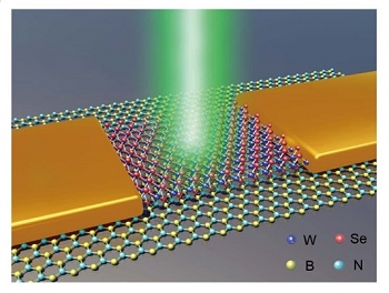
NUS scientists have developed multibit optoelectronic memory using a heterostructure made of two-dimensional (2D) materials for next generation devices.
Optoelectronic memories are devices which can store photon-generated charge carriers when exposed to light. The stored charges can be accessed later for information retrieval. These devices can be used in image capture and spectrum analysis systems. 2D atomically layered materials are promising candidates for the development of next generation optoelectronic memories to meet emerging requirements for device miniaturisation and structural flexibility. However, optoelectronic memories fabricated using 2D materials have been reported to suffer from poor data storage capability with the highest reported figure at about eight distinct storage states.
A team lead by Prof CHEN Wei from both the Department of Chemistry and the Department of Physics, NUS has developed a multibit, non-volatile optoelectronic memory device that is able to store up to 130 distinct states by using a tungsten diselenide/ boron nitride (WSe2/ BN) heterostructure. The heterostructure, made of 2D materials, comprises a monolayer of WSe2 on a 20-layer BN. The programming (store data) and erasing (delete data) functions are controlled by adjusting the applied polarity to the device. A negative polarity is applied during the programming function and it causes the photon-generated electrons from the midgap donor-like states of the BN material to transfer into the WSe2 material. This leaves behind localised (non-mobile) positive charges in the BN material. For the erasing function, a positive polarity is applied. This causes the photon-generated electrons from the valence band in the BN material to recombine with the localised positive charges, returning it to a neutral state.
The amount of electrons transferred into the WSe2 material is dependent on the duration of light exposure time for the device. A longer exposure time would mean that more electrons are transferred. The researchers found that the continual accumulation of electrons in the WSe2 material corresponding up to 130 light pulses can be detected before saturation conditions set in. Each of these pulses can be treated as a distinct storage state. During performance testing, they found that the device exhibits a data retention of over 4.5×10⁴ seconds and a cyclic programme/ erase endurance exceeding 200 cycles.
Explaining the significance of the findings, Prof Chen said, “Although there is still a performance gap when compared to commercial silicon-based memory, these devices are advantageous in electronic applications which require structural flexibility. The use of this WSe2/ BN 2D layered heterostructure provides a method to achieve multibit memory device and may pave the way for the development of next generation optoelectronic memories.”
Share on:


Suggested Items
Real Time with... IPC APEX EXPO 2024: Sustainability in the Industry
04/26/2024 | Real Time with...IPC APEX EXPOGuest Editor Henry Crandall and Chris Nash of Indium Corporation discuss the company's 90th anniversary and its focus on sustainability. They focus on the benefits of sustainable materials, their compatibility, and value propositions. The conversation also highlights how Durafuse LT technology's role in reducing reflow temperatures is leading to significant cost and energy savings. Nash also touches on downstream sustainability efforts such as using recycled materials for packaging.
SMC Korea 2024 to Highlight Semiconductor Materials Trends and Innovations on Industry’s Path to $1 Trillion
04/24/2024 | SEMIWith Korea a major consumer of semiconductor materials and advanced materials a key driver of innovation on the industry’s path to $1 trillion, industry leaders and experts will gather at SMC (Strategic Materials Conference) Korea 2024 on May 29 at the Suwon Convention Center in Gyeonggi-do, South Korea to provide insights into the latest materials developments and trends. Registration is open.
Groundbreaking Ceremony Marks the Beginning of a New Era for Newccess Industrial; The Construction of the MINGXIN Building
04/12/2024 | Newccess IndustrialOn a clear and sunny day in March, the groundbreaking ceremony for the MINGXIN Building took place in Shenzhen, China. This moment marked the official commencement of construction for a project that will reshape the semiconductor materials industry.
The Need for a Holistic Global Sustainability Standard
04/10/2024 | Michael Ford, Aegis SoftwareNo one can deny that the resources of our fragile planet are finite. The environment seems like a third party, subject to constant degradation. We’re acutely aware of the effects of pollution on our climate, and despite our “throw-away” culture, recycling and recovery of materials has remained relatively expensive, even as we use more energy just to survive.
iNEMI Publishes Four Roadmap Topics
04/04/2024 | iNEMIThe International Electronics Manufacturing Initiative (iNEMI) announces the availability of the first roadmap topics in the new iNEMI Roadmap format. Printed circuit boards, sustainable electronics, smart manufacturing, and mmWave materials and test are now available online.