


 The Right Approach: I Hear the Train A Comin'
 It’s Only Common Sense: OCCAM—the Time Is Now
 Marcy's Musings: The Growing Industry
Efficient Light Conversion with Perovskite Nanocrystals
October 12, 2018 | University of AmsterdamEstimated reading time: 3 minutes
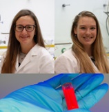
Perovskites are a family of crystals that show promising properties for applications in nano-technology. However, one useful property that until now was unobserved in perovskites is so-called carrier multiplication—an effect that makes materials much more efficient in converting light into electricity. New research, led by UvA-IoP physicists Dr Chris de Weerd and Dr Leyre Gomez from the group of Prof. Tom Gregorkiewicz, has now shown that certain perovskites in fact do have this desirable property.
Crystals are configurations of atoms, molecules or ions, that are ordered in a structure that repeats itself in all directions. We have all encountered some crystals in everyday life: ordinary salt, diamond and even snowflakes are examples. What is perhaps less well-known is that certain crystals show very interesting properties when their size is not that of our everyday life but that of nanometers—a few billionths of a meter. There, we enter the world of nanocrystals, structures that have shown to be extremely useful in constructing technological applications at tiny scales.
Perovskites—named after 19th century Russian mineralogist Lev Perovski—form a particular family of materials that all share the same crystal structure. These perovskites have many desirable electronic properties, making them useful for constructing for example LEDs, TV-screens, solar cells and lasers. For this reason, the perovskites have been studied extensively by physicists in the past years.
Carrier Multiplication
A property which so far had not been shown to exist in perovskites is carrier multiplication. When semiconductors—in solar cells, for example—convert the energy of light into electricity, this is usually done one particle at a time: a single infalling photon results in a single excited electron (and the corresponding ‘hole’ where the electron used to be) that can carry an electrical current. However, in certain materials, if the infalling light is energetic enough, further electron-hole pairs can be excited as a result; it is this process that is known as carrier multiplication.
When carrier multiplication occurs, the conversion from light into electricity can become much more efficient. For example, in ordinary solar cells there is a theoretical limit (the so-called Shockley-Queisser limit) on the amount of energy that can be converted in this way: at most a little over 33% of the solar power gets turned into electrical power. In semiconductor nanocrystals that feature the carrier multiplication effect, however, a maximum efficiency of up to 44% is predicted.
PhD
This makes it very interesting to search for the carrier multiplication effect in perovskites as well, and that is precisely what UvA-IoP physicists Chris de Weerd and Leyre Gomez from the Optoelectronic Materials group led by Prof. Tom Gregorkiewicz, in collaboration with the group of Prof. Yasufumi Fujiwara and with support of their colleagues from the AIST National Institute in Tsukuba and the Delft University of Technology have now done. Using spectroscopy methods—studying the frequencies of the radiation that comes from a material after very briefly illuminating it with a flash of light—the researchers showed that perovskite nanocrystals made out of cesium, lead and iodine, do indeed display carrier multiplication. Moreover, they argue that the efficiency of this effect is higher than reported thus far for any other materials; with this finding therefore, the extraordinary properties of perovskites receive a new boost.
De Weerd, who successfully defended her PhD thesis based on this and other research last week, says: “Until now, carrier multiplication had not been reported for perovskites. That we have now found it is of great fundamental impact on this upcoming material. For example, this shows that perovskite nanocrystals can be used to construct very efficient photodetectors, and in the future perhaps solar cells.”
Share on:


Suggested Items
Real Time with... IPC APEX EXPO 2024: Sustainability in the Industry
04/26/2024 | Real Time with...IPC APEX EXPOGuest Editor Henry Crandall and Chris Nash of Indium Corporation discuss the company's 90th anniversary and its focus on sustainability. They focus on the benefits of sustainable materials, their compatibility, and value propositions. The conversation also highlights how Durafuse LT technology's role in reducing reflow temperatures is leading to significant cost and energy savings. Nash also touches on downstream sustainability efforts such as using recycled materials for packaging.
SMC Korea 2024 to Highlight Semiconductor Materials Trends and Innovations on Industry’s Path to $1 Trillion
04/24/2024 | SEMIWith Korea a major consumer of semiconductor materials and advanced materials a key driver of innovation on the industry’s path to $1 trillion, industry leaders and experts will gather at SMC (Strategic Materials Conference) Korea 2024 on May 29 at the Suwon Convention Center in Gyeonggi-do, South Korea to provide insights into the latest materials developments and trends. Registration is open.
Groundbreaking Ceremony Marks the Beginning of a New Era for Newccess Industrial; The Construction of the MINGXIN Building
04/12/2024 | Newccess IndustrialOn a clear and sunny day in March, the groundbreaking ceremony for the MINGXIN Building took place in Shenzhen, China. This moment marked the official commencement of construction for a project that will reshape the semiconductor materials industry.
The Need for a Holistic Global Sustainability Standard
04/10/2024 | Michael Ford, Aegis SoftwareNo one can deny that the resources of our fragile planet are finite. The environment seems like a third party, subject to constant degradation. We’re acutely aware of the effects of pollution on our climate, and despite our “throw-away” culture, recycling and recovery of materials has remained relatively expensive, even as we use more energy just to survive.
iNEMI Publishes Four Roadmap Topics
04/04/2024 | iNEMIThe International Electronics Manufacturing Initiative (iNEMI) announces the availability of the first roadmap topics in the new iNEMI Roadmap format. Printed circuit boards, sustainable electronics, smart manufacturing, and mmWave materials and test are now available online.