


 Elementary, Mr. Watson: High Power: When Physics Becomes Real
 The Shaughnessy Report: Watt About Power Integrity?
 Global PCB Connections: Understanding Your Fabricator’s Capabilities (or Niche)


Calculation of Frequency-Dependent Effective Roughness Dielectric Parameters for Copper Foil Using Equivalent Capacitance Models
January 2, 2019 | Marina Y. Koledintseva, Metamagnetics Inc.*, and Tracey Vincent, CST of AmericaEstimated reading time: 20 minutes
Printed circuit boards (PCBs) used in high-speed digital design are known to have a substantial level of copper foil roughness which compromises signal integrity (SI) and may also cause electromagnetic compatibility (EMC) problems. Therefore, knowledge of the correct parameters of laminate PCB dielectrics refined from any copper foil roughness impact and the proper foil roughness characterization are important constituents of modeling high-speed digital electronics designs, see, e.g., [1,2,3] and references therein.
The Effective Roughness Dielectric (ERD) concept was introduced in [4,5,6]. ERD is a homogeneous lossy dielectric layer of certain thickness Tr with effective (averaged) dielectric constant DKr and dissipation factor DFr. ERD is placed on a smooth conductor surface to substitute an inhomogeneous transition layer between a conductor and laminate substrate dielectric. While the concept is simple, it is physically illuminating, meaningful, and powerful. It has been successfully applied to model conductor (copper foil) roughness in printed circuit boards for signal integrity (SI) and electromagnetic interference (EMI) purposes when designing high-speed digital electronics devices [7,8]. The ERD model has been implemented and tested in a number of numerical electromagnetic modeling tools, see, e.g., [9,10,11,12].
In our previous publications [6,13,14], the ERD “design curves”, determining the ranges of the DKr and DFr parameters for different types of PCB copper foils, were developed. The methodology of generating these “design curves” is based on the following procedures:
- Stripline S-parameter Sweep (S3) technique to measure S-parameters of single-ended comparatively long (~40 cm, or 16 inches) striplines with TRL calibration to remove connector effects [15,16];
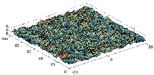
- Scanning Electron Microscopy (SEM) or high-resolution optical microscopy of cross-sections of PCB samples with signal traces and the proper quantification of surface roughness profile parameters [17,18,19];
- Differential Extrapolation Roughness Measurement (DERM) technique [20,21,22]; and
- 2D-FEM and/or 3D FIT numerical modeling that allow for accurately fitting the measured S-parameters of the striplines and extract the data for DKr and DFr of the roughness layers [4,6,13,14]. This fitting may include an optimization procedure, e.g., a genetic algorithm, to minimize the discrepancy between the modeled and measured S-parameters.
The "design curves" in the abovementioned papers were generated using SEM and/or optical microscopy to quantify foil roughness. Any designer can use these “design curves” and does not necessarily need to cut a PCB and prepare samples of the lines cross-sections for microscopic inspection. It is sufficient to know which type of foil is used in the PCB under test – this may be standard (STD) foil, VLP (very low profile), RTF (reverse-treated foil), or HVLP (hyper-very low profile)/ SVLP (super-very low profile) foil. Each foil type (group) has some ranges of DKr, DFr, and Tr values, and a designer may take average values DKr, DFr, and Tr within these ranges for the reasonable estimation of the data which then could be used in modeling of the PCB designs.
Although the “design curves” were developed using fitting between the experimental data and modeling results, it is always desirable to have an analytical model. In this work, the DKr and DFr parameters are derived based on the understanding that the transition layer between the dielectric and foil contains gradual variation of concentration of metallic inclusions: from zero concentration in laminate dielectric through some percolation limit to 100% at the smooth copper foil level. The equivalent material parameters of this layered structure can be obtained using equivalent capacitance approach. In the equivalent capacitor the dielectric properties vary gradually according to the concentration profile of metallic particles in the roughness layer. The concentration profile can be obtained from SEM or high-resolution optical microscopy. As concentration of metallic particles increases along the axis normal to the laminate dielectric and foil boundary, two regions can be determined: insulating (pre-percolation) and conducting (percolation). Rates of increase of effective loss (or effective conductivity) in these two regions significantly differ. The proposed model of equivalent capacitance with gradient dielectric has been applied to STD and VLP foils, and the results are validated using 3D numerical electromagnetic simulations.
Description of Equivalent Capacitance Model
A roughness profile on a PCB conductor surface can be tested using optical or SEM microscopy, or a surface profiler. The average contents (volume concentration) of metallic particles in the roughness layer varies as a function of the coordinate z normal to the surface. It can be approximated by an exponential function,
(1)
where a and K1 are the fitting parameters.
Two separate regions of effective roughness dielectric can be considered:
Region I: 0p, where the concentration of metallic inclusions is below the percolation threshold, i.e., where the mixture remains in the dielectric phase; this is the region adjacent to the dielectric matrix of the PCB. Herein, Tp is the distance within the layer at which percolation is reached.
Region II: Tp, where the concentration of metallic inclusions is higher than the percolation threshold; this is the region adjacent to the smooth foil level and is conducting. Herein, T is the entire thickness of ERD layer. It includes,
(2)
where ΔT is the thickness of the region above the percolation.
The concentration , at which percolation will occur for the metallic particles in the roughness dielectric layer, can be obtained empirically, i.e., estimated from the microscopy pictures, or from the profiler data. By solving the equation,
(3)
with respect to Tp, one can get the height of the dielectric phase of ERD.
First, let us consider the region 0p. This is the dielectric layer with relative permittivity varying according to the profile function (1) from the matrix dielectric properties em (at z=0) to the final pre-percolation value ep (at z=Tp). Since dielectric function varies with z as,
(4)
The effective permittivity of such a layer can be calculated through the equivalent partial layered capacitor consisting of series connection of sublayer capacitors. The capacitance of the resultant capacitor with variable properties of the dielectric is,
(5)
where C0 is the capacitance of the corresponding air-filled rectangular parallel-plate capacitor of thickness, d. Herein, d = Tp.
The effective dielectric properties of such dielectric layer can be easily derived from (5) as
(6)
Page 1 of 4
Share on:


Testimonial
"Advertising in PCB007 Magazine has been a great way to showcase our bare board testers to the right audience. The I-Connect007 team makes the process smooth and professional. We’re proud to be featured in such a trusted publication."
Klaus Koziol - atgSuggested Items
Episode 6 of Ultra HDI Podcast Series Explores Copper-filled Microvias in Advanced PCB Design and Fabrication
10/15/2025 | I-Connect007I-Connect007 has released Episode 6 of its acclaimed On the Line with... American Standard Circuits: Ultra High Density Interconnect (UHDI) podcast series. In this episode, “Copper Filling of Vias,” host Nolan Johnson once again welcomes John Johnson, Director of Quality and Advanced Technology at American Standard Circuits, for a deep dive into the pros and cons of copper plating microvias—from both the fabricator’s and designer’s perspectives.
Nolan’s Notes: Tariffs, Technologies, and Optimization
10/01/2025 | Nolan Johnson -- Column: Nolan's NotesLast month, SMT007 Magazine spotlighted India, and boy, did we pick a good time to do so. Tariff and trade news involving India was breaking like a storm surge. The U.S. tariffs shifted India from one of the most favorable trade agreements to the least favorable. Electronics continue to be exempt for the time being, but lest you think that we’re free and clear because we manufacture electronics, steel and aluminum are specifically called out at the 50% tariff levels.
MacDermid Alpha & Graphic PLC Lead UK’s First Horizontal Electroless Copper Installation
09/30/2025 | MacDermid Alpha & Graphic PLCMacDermid Alpha Electronics Solutions, a leading supplier of integrated materials and chemistries to the electronics industry, is proud to support Graphic PLC, a Somacis company, with the installation of the first horizontal electroless copper metallization process in the UK.
Electrodeposited Copper Foils Market to Grow by $11.7 Billion Over 2025-2032
09/18/2025 | Globe NewswireThe global electrodeposited copper foils market is poised for dynamic growth, driven by the rising adoption in advanced electronics and renewable energy storage solutions.
MacDermid Alpha Showcases Advanced Interconnect Solutions at PCIM Asia 2025
09/18/2025 | MacDermid Alpha Electronics SolutionsMacDermid Alpha Electronic Solutions, a global leader in materials for power electronics and semiconductor assembly, will showcase its latest interconnect innovations in electronic interconnect materials at PCIM Asia 2025, held from September 24 to 26 at the Shanghai New International Expo Centre, Booth N5-E30