


 The Right Approach: I Hear the Train A Comin'
 It’s Only Common Sense: OCCAM—the Time Is Now
 Marcy's Musings: The Growing Industry
Scientists Create New Class of Two-Dimensional Materials
June 10, 2019 | University of California, IrvineEstimated reading time: 2 minutes
In a paper published this week in Nature, materials science researchers at the University of California, Irvine and other institutions unveil a new process for producing oxide perovskite crystals in exquisitely flexible, free-standing layers.
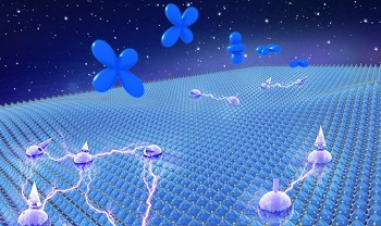
Image Caption: “Through our successful fabrication of ultrathin perovskite oxides down to the monolayer limit, we’ve created a new class of two-dimensional materials,” says Xiaoqing Pan, professor of materials science & engineering and Henry Samueli Endowed Chair in Engineering at UCI. “Since these crystals have strongly correlated effects, we anticipate they will exhibit qualities similar to graphene that will be foundational to next-generation energy and information technologies.” Xiaoqing Pan / UCI
A two-dimensional rendition of this substance is intriguing to scientists and engineers, because 2D materials have been shown to possess remarkable electronic properties, including high-temperature superconductivity. Such compounds are prized as potential building blocks in multifunctional high-tech devices for energy and quantum computing, among other applications.
“Through our successful fabrication of ultrathin perovskite oxides down to the monolayer limit, we’ve created a new class of two-dimensional materials,” said co-author Xiaoqing Pan, professor of materials science & engineering and Henry Samueli Endowed Chair in Engineering at UCI. “Since these crystals have strongly correlated effects, we anticipate they will exhibit qualities similar to graphene that will be foundational to next-generation energy and information technologies.”
For all of their promising physical and chemical properties, oxide perovskites are difficult to render in flat layers due to the clunky, strongly bonded structure of their crystals. Earlier efforts at making free-standing, monolayer films of the material through the pulsed laser deposition method failed.
Pan’s cross-disciplinary group of researchers applied a technique called molecular beam epitaxy to grow the thin oxide films layer by layer on a template with a water-dissolvable buffer, followed by etching and transfer.
“Most of the known two-dimensional materials can be synthesized by exfoliation or by chemical deposition, as their bulk crystals consist of unique layered structures in which many strong covalently bonded planes are held together by weak van der Waals interactions,” he said. “But oxide perovskite is different; like most oxide materials, it has strong chemical bonds in three dimensions, making it especially challenging to fabricate into two dimensions.”
Pan, who holds a dual appointment as a professor of physics & astronomy and directs the Irvine Materials Research Institute, said that molecular beam epitaxy is a more precise method for growing oxide perovskite thin films with almost no defects. He knows this because his research team was able to review its work at atomic resolution using aberration-corrected transmission electron microscopy.
“TEM played a crucial role in this project, because it provided important feedback for the optimization of film growth conditions and allowed us to directly observe novel phenomena, including the crystal symmetry breaking and unexpected polarization enhancement under the reduced dimension,” Pan said.
“Given the outstanding physical and chemical properties of oxide perovskites and novel phenomena emergent at the monolayer limit, this work opens new possibilities in the exploration of quantum behaviors in strongly correlated two-dimensional materials,” he added.
Pan and his team at UCI were joined by collaborators at China’s Nanjing University and the University of Nebraska. They used TEM facilities at UCI’s Irvine Materials Research Institute. The project was supported by the U.S. Department of Energy Office of Basic Energy Sciences’ materials sciences and engineering division, under grant DE-SC0014430.
Share on:


Suggested Items
Real Time with... IPC APEX EXPO 2024: Sustainability in the Industry
04/26/2024 | Real Time with...IPC APEX EXPOGuest Editor Henry Crandall and Chris Nash of Indium Corporation discuss the company's 90th anniversary and its focus on sustainability. They focus on the benefits of sustainable materials, their compatibility, and value propositions. The conversation also highlights how Durafuse LT technology's role in reducing reflow temperatures is leading to significant cost and energy savings. Nash also touches on downstream sustainability efforts such as using recycled materials for packaging.
SMC Korea 2024 to Highlight Semiconductor Materials Trends and Innovations on Industry’s Path to $1 Trillion
04/24/2024 | SEMIWith Korea a major consumer of semiconductor materials and advanced materials a key driver of innovation on the industry’s path to $1 trillion, industry leaders and experts will gather at SMC (Strategic Materials Conference) Korea 2024 on May 29 at the Suwon Convention Center in Gyeonggi-do, South Korea to provide insights into the latest materials developments and trends. Registration is open.
Groundbreaking Ceremony Marks the Beginning of a New Era for Newccess Industrial; The Construction of the MINGXIN Building
04/12/2024 | Newccess IndustrialOn a clear and sunny day in March, the groundbreaking ceremony for the MINGXIN Building took place in Shenzhen, China. This moment marked the official commencement of construction for a project that will reshape the semiconductor materials industry.
The Need for a Holistic Global Sustainability Standard
04/10/2024 | Michael Ford, Aegis SoftwareNo one can deny that the resources of our fragile planet are finite. The environment seems like a third party, subject to constant degradation. We’re acutely aware of the effects of pollution on our climate, and despite our “throw-away” culture, recycling and recovery of materials has remained relatively expensive, even as we use more energy just to survive.
iNEMI Publishes Four Roadmap Topics
04/04/2024 | iNEMIThe International Electronics Manufacturing Initiative (iNEMI) announces the availability of the first roadmap topics in the new iNEMI Roadmap format. Printed circuit boards, sustainable electronics, smart manufacturing, and mmWave materials and test are now available online.