


 Powering the Future: Why Thermal Management Defines the Future of Electronics
 Standard of Excellence: Engineering Is the New Sales—How Technical Collaboration Wins Business
 SMT Perspectives & Prospects: Artificial Intelligence, Part 7—Data Module 2


The Role of Parylene Conformal Coatings in Next-gen Electronics
August 19, 2019 | Tim Seifert, Specialty Coating SystemsEstimated reading time: 3 minutes
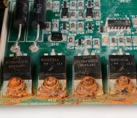
Designers and manufacturers of electronics are under pressure to make packages smaller, lighter, and more environmentally friendly. They also need to ensure that their new technologies perform reliably in their operating environments, which may include exposure to chemicals, moisture, electrical charges, and extreme temperatures while maintaining compliance to a growing number of stringent environmental, safety, industry-specific, governmental, and/or biological regulations. In this article, I will take a closer look at Parylene conformal coatings and the role they can play in helping manufacturers address current and future challenges in the electronics industry.
Developed by Union Carbide scientists in the late 1950s, Parylene is the generic name for a unique series of polymeric organic coating materials. They are polycrystalline and linear in nature, possess useful dielectric and barrier properties per unit thickness, and are chemically inert. Parylene coatings are ultra-thin, pinhole-free, and truly conform to components due to their molecular level polymerization— basically “growing” on the substrate surface one molecule at a time.
Parylene coatings are applied in a vapor deposition process rather than by dispensing, spraying, brushing, or dipping. The process begins by placing parts to be coated in the deposition chamber. The powdered raw material—known as “dimer”—is then placed in the vaporizer at the opposite end of the system. The dimer is heated, causing it to sublimate to a vapor, and then heated again to break it into a monomeric vapor. This vapor is transferred into an ambient temperature chamber where it spontaneously polymerizes onto the parts, forming the thin Parylene film. The Parylene deposition process is carried out in a closed system under a controlled vacuum with the deposition chamber remaining at room temperature throughout the entire process. No solvents, catalysts, or plasticizers are used in the coating process.
Because there is no liquid phase in this deposition process, there are no subsequent meniscus, pooling, or bridging effects as seen in the application of liquid coatings; thus, the entire part is equally protected. The molecular “growth” of Parylene coatings also ensures not only an even, conformal coating at the thickness specified by the manufacturer, but because Parylene is formed from a gas, it also penetrates into every crevice—regardless of how seemingly inaccessible. This ensures complete encapsulation of the substrate without blocking small openings.
Additionally, Parylene coatings are extremely lightweight, offering excellent barrier properties without adding dimension or significant mass to delicate components. Typical Parylene coatings range in thickness from 500 angstroms to 75 microns. Most other coating materials cannot be applied as thin as Parylene and still provide the same level of protection.
There are several variants in the poly-paraxylylene family, but all are completely linear, highly crystalline materials that provide the benefits of being ultra-thin and lightweight. They all also provide an excellent dielectric, moisture, and chemical barrier, add strength to wire bonds, ensure efficient signal transmission, and are biocompatible. Parylenes have extremely low dielectric constants and dissipation factors, enabling them to provide small, tight packages with dielectric insulation via a thin coating. The voltage breakdown per unit thickness actually increases with decreasing Parylene film thickness.
Parylene coatings have been used throughout the electronics, transportation, aerospace, defense, and medical device industries for over 45 years to solve industry challenges. In fact, where other solutions have become insufficient to meet the growing needs of the industry, Parylene coatings are providing answers at a time when products need to be small, lightweight, robust, and reliable.
Industry Challenges and the Parylene Solution
Small and Lightweight
Whether working on gadgets for the consumer market or defense hardware, electronics manufacturers face relentless pressure to make electronic packages smaller and lightweight; this is a constant, regardless of the size of the overall device. While mobile phones have actually become larger in recent years, they are packed with more power and functionality than their predecessors so their internal components had to shrink. Similarly, automobiles and aircraft stay roughly the same size, but additional electronic components are used to increase their functionality and reliability. At the same time, there is an increasing call in these industries to reduce weight to improve system efficiencies.
Because Parylene coatings are applied as a vapor, the molecules grow into a film, adhering equally to every surface and edge and within crevices. The coatings completely encapsulate complex substrates, providing excellent barrier and dielectric protection. Additionally, due to their ultra-thin nature, the protection they provide is achieved without adding significant dimension or mass.
Comparatively, liquid coatings are commonly applied by spray, brush, or dip and may not provide complete coverage due to pooling, bridging, or meniscus effects. While these coating solutions may be sufficient for some applications, they have their limitations when it comes to today’s advanced electronic designs.
To read the full article, which appeared in the August 2019 issue of SMT007 Magazine, click here.
Share on:


Testimonial
"We’re proud to call I-Connect007 a trusted partner. Their innovative approach and industry insight made our podcast collaboration a success by connecting us with the right audience and delivering real results."
Julia McCaffrey - NCAB GroupSuggested Items
Spirit Electronics Named Authorized Distributor for Microchip Technology
04/17/2026 | Globe NewswireSpirit Electronics, a vertically integrated electronics design and manufacturing solutions provider serving the military and aerospace markets, announced that it has been designated as an authorized distributor for the Americas for Microchip Technology, a broadline supplier of semiconductors committed to making innovative design easier through total system solutions.
FTG Reports Strong Q1 2026 Results with Double-Digit Revenue Growth and Rising Backlog
04/09/2026 | Firan Technology Group CorporationIn Q1 2026, the Corporation grew organically. FTG is strategically investing its capital in ways that will drive increased shareholder returns for the future in both the near term and long term. The company's achievements in Q1 2026 demonstrate this commitment, laying a strong foundation for future growth.
EMI Promotes David Vue to Lead Military and Aerospace Division
03/31/2026 | Express Manufacturing Inc.Express Manufacturing, Inc. (EMI), a global electronics manufacturing services (EMS) provider, announced the promotion of David Vue to Military and Aerospace Division Manager.
SP Manufacturing Expands into UK Avionics Sector, Secures First Customer Engagement
03/30/2026 | SP ManufacturingSP Manufacturing Pte Ltd., a leader in comprehensive electronic manufacturing services, announced its expansion into the avionics sector in the United Kingdom, marked by the successful onboarding of its first UK-based avionics customer.
Honeywell Aerospace, Defense Department Sign Deal to Boost Defense Tech Production
03/27/2026 | PRNewswireHoneywell announced it has signed a groundbreaking supplier framework agreement with the U.S. Department of War (DoW) to rapidly increase the production of critical defense technologies. This agreement includes a $500 million multi-year investment to upgrade the company's production capacity.