


 The Pulse: Caught in the Crosshatch—A Cautionary Tale of Detective Work
 Fresh PCB Concepts: Designing PCBs for Harsh Environments—Reliability Is Engineered Upstream
 Elementary, Mr. Watson DFX—Basically a Basket of Crabs With Spreadsheets


Ambarella Adopts Cadence Clarity 3D Solver for AI Vision Processor Development
June 1, 2020 | Business WireEstimated reading time: 1 minute
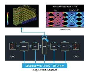
Cadence Design Systems, Inc. announced that Ambarella, Inc. has adopted the Cadence Clarity 3D Solver for design of their next-generation AI vision processors.
Ambarella’s products are used in a wide variety of human and computer vision applications, including video security, advanced driver assistance systems (ADAS), electronic mirror, drive recorder, driver/cabin monitoring, autonomous driving and robotic applications.
Per a recent evaluation, an Ambarella computer vision (CV) system on chip (SoC) and PCB were run on the Cadence Clarity 3D Solver. Results of both simulations show that when there is no solid reference plane for high-speed signals, the Clarity 3D Solver identifies the Ambarella design defects and correct scattering parameter (S-parameter) response. For both simulations, the Clarity 3D Solver, a 3D electromagnetic solver using 32 CPUs, took just 29 hours to process the case with 202 ports running at 48 bits via a LPDDR4 interface on a geometrical combination of package and PCB layout design.
“Ambarella continuously upgrades our system design methodologies to stay ahead of the competition,” said Chan Lee, vice president of VLSI at Ambarella, Inc. “The speed, capacity and accuracy of the Cadence Clarity 3D Solver enable us to accelerate our design process and shorten our schedule. We expect that many of the likely challenges of our next-generation 5nm AI design project can be easily and quickly addressed with the Cadence Clarity 3D Solver.”
The Clarity 3D Solver harnesses state-of-the-art distributed multiprocessing technology to efficiently tackle electromagnetic (EM) challenges encountered when designing complex 3D structures. The innovative Clarity 3D Solver is integrated with Cadence’s chip, package and PCB design solutions as part of Cadence’s Intelligent System Design™ strategy.
Share on:


Testimonial
"The I-Connect007 team is outstanding—kind, responsive, and a true marketing partner. Their design team created fresh, eye-catching ads, and their editorial support polished our content to let our brand shine. Thank you all! "
Sweeney Ng - CEE PCBSuggested Items
Zuken Launches GENESYS 2026 to Broaden Access and Improve MBSE Workflows
04/28/2026 | ZukenZuken announced GENESYS 2026, the latest version of its model-based systems engineering platform, with updates designed to improve performance, expand access to model-based information, and enhance the day-to-day modeling experience for engineering teams.
EDADOC: Building the ‘Neural Hub’ for High-Compute Chips Within a Compact Space
04/28/2026 | ECIOEvery chip to the market must pass a stringent checkpoint before shipment known as ATE testing. Serving as the physical “neural hub” that connects test equipment worth millions of dollars with the device under test, the performance of the ATE test board directly determines the accuracy, efficiency, and final yield of chip testing. Amid the rapid rise of high-compute chips, what extreme challenges is this seemingly small circuit board facing? How is EDADOC addressing industry pain points through its one-stop “design + manufacturing” model?
Cadence Reports Q1 2026 Financial Results
04/28/2026 | Cadence Design SystemsCadence had a strong start to 2026, delivering a solid Q1 with accelerating AI demand and record backlog, reflecting strong customer commitment to our AI-driven portfolio,” said Anirudh Devgan, president and chief executive officer.
Tomachie Launches AI-Powered PCB Analysis with Smart Test Point Insertion
04/28/2026 | TomachieTomachie announced its AI-Assisted PCB schematic design analysis platform, enabling engineering teams to evaluate and improve schematic quality before layout begins. Schematic errors caught after layout — or in production — cost 10 to 100 times more to fix than those caught during schematic capture.
The Pulse: Caught in the Crosshatch—A Cautionary Tale of Detective Work
04/29/2026 | Martyn Gaudion -- Column: The PulseA chance meeting at a family wedding the other week led to a conversation about numbers, an introduction to a book entitled Humble Pi, and how numeric misinterpretation can lead to all kinds of unexpected outcomes, some just costly, others tragic. It’s a good and amusing read, and as a result of this conversation with someone I had previously never met, I feel somewhat (at least temporarily) enlightened. One of the takeaways of the book is that humans are born to think logarithmically, and linear math has to be formally educated into our brains. That got me curious for more.