


 The Marketing Minute: If Your Marketing Budget Gets Cut in Half, Then What?
 Punching Out: How Are the Big Boys in Electronics Doing?
 It’s Only Common Sense: Complexity Is the Enemy of Profit


MKS Introduces ESI Geode A CO2 Laser System for High Precision and High-Speed ABF IC Substrate Manufacturing
May 31, 2023 | MKS Instruments, Inc.Estimated reading time: 1 minute
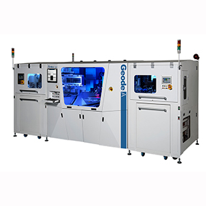
MKS Instruments, Inc., a global provider of technologies that transform our world, announced the official launch of the ESI Geode® A laser drill system today, a new configuration of the Geode® platform designed explicitly for drilling vias in the non-copper-clad ABF substrate market.
The Geode® A laser drilling system provides processing and application solutions for the FCBGA package substrate market, components which provide critical building blocks for everyday electronic devices and, in particular, high-performance computing. FCBGA substrates help enable supercomputing, artificial intelligence processing, autonomous cars, and other highly complex semiconductor modules.
“Manufacturers are under increased market pressure to deliver components that meet the precise demands of miniaturization and complexity required for advanced substrate manufacturing. At MKS, we are keenly focused on delivering the advanced technology needed for our customers to deliver next-generation productivity and quality,” said John Williams, MKS Vice President and General Manager of the ESI business. “In addition, the Geode® A laser drill is engineered as an integral component to the MKS Optimize the Interconnect SM solution, combining ESI laser drilling technologies with Atotech chemistry and plating equipment to provide customers with a full package of via formation technologies required to deliver optimal quality with the highest productivity for PCB and package substrate products.”
The Geode® A laser drilling system combines an innovative laser and optics configuration with precision pulse-shaping and beam-steering designed for ABF materials. These engineering innovations deliver the lowest cost of ownership and a greener manufacturing solution through 21% less floor space utilization, 72% less weight, and up to 65% less power consumption than the competition.
The Geode® A laser drilling system is available for purchase. More details can be found at www.esi.com, and system experts will be available at the JPCA 2023, Tokyo, Japan, May 31-June 2 in booth 6B-11.
Share on:


Testimonial
"Our marketing partnership with I-Connect007 is already delivering. Just a day after our press release went live, we received a direct inquiry about our updated products!"
Rachael Temple - AlltematedSuggested Items
I-Connect007 Releases The Printed Circuit Designer’s Guide to… Direct Metallization: A Guide to Complex PCB Fabrication
05/15/2026 | I-Connect007As PCB complexity continues to accelerate, fabricators and OEMs are reevaluating long-standing manufacturing processes to meet the demands of AI, HDI, advanced packaging, and next-generation electronics. To address these evolving challenges, I-Connect007 is proud to announce the release of The Printed Circuit Designer’s Guide to… Direct Metallization: A Guide to Complex PCB Fabrication, authored by MacDermid Alpha Solution’s Carmichael Gugliotti.
Driving Innovation: Selecting the Right Laser Source
04/28/2026 | Simon Khesin -- Column: Driving InnovationWhen I first joined Schmoll Maschinen, I brought experience from almost every PCB process, except for laser. As I immersed myself in laser processing, I realized why it can seem so daunting to a newcomer. The complexity arises from three intersecting factors: A vast variety of laser sources: CO2, UV-nano, green-pico, UV-pico, IR-pico, and others; a diverse range of applications: Drilling, cutting, ablation, and more; and an extensive list of materials: These have vastly different absorption rates. Choosing the right machine or laser source is rarely trivial. Even for experienced engineers, answering "Which source is best?" requires examining the business's specific goals.
Institute of Circuit Technology Spring Seminar 2026: A Bright Future in Europe
04/23/2026 | Pete Starkey, I-Connect007Through the leafy lanes and spring flowers of Warwickshire and back to Meridan, the traditional centre of England, and now officially part of the Metropolitan Borough of Solihull in the county of the West Midlands, I attended the Annual General Meeting and Spring Seminar of the Institute of Circuit Technology (ICT) on April 14. Out of the AGM came notable changes in leadership at the top of the Institute: the retirement of Mat Beadel as chair and Emma Hudson as technical director. Effective May 1, Steve Driver is the new chair, and Alun Morgan is the new technical director.
ACCM Unveils Negative and Near-zero CTE Materials for Large-Format AI Chips
04/21/2026 | Advanced Chip and Circuit MaterialsAdvanced Chip and Circuit Materials, Inc. (ACCM) has launched two new materials: Celeritas HM50, with a negative coefficient of thermal expansion (CTE) of -8 ppm/°C to offset the positive CTE and expansion of copper with temperature on circuit boards, and Celeritas HM001, with near-zero CTE and the low-loss performance needed for high-speed signal layers to 224 Gb/s and faster in artificial intelligence (AI) circuits.
Fresh PCB Concepts: Designing PCBs for Harsh Environments—Reliability Is Engineered Upstream
04/23/2026 | Team NCAB -- Column: Fresh PCB ConceptsWhen engineers hear the phrase “harsh environment,” they usually think of the extreme temperature swings, vibration and shock, pressure changes, or radiation in aerospace. However, aerospace is not the only harsh environment where electronic assemblies must survive. Automotive power electronics, downhole oil and gas tools, marine controls, rail systems, defense platforms, and industrial automation equipment all expose PCBs to environments that are equally unforgiving. The stress mechanisms may differ, but the physics does not.