














 Target Condition: The Modern Masters of Signal Integrity and AI-driven Design
 Fresh PCB Concepts: Repair and Risk in Electrical Test Failures in PCB Manufacturing
 Elementary, Mr. Watson: The Design Matrix—Revealing the Hidden Truths of Reality






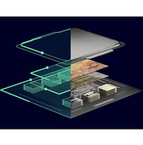
The walls are coming down between the designers of chips and PCBs. Because of the complexity of electronic systems, IC designers and PCB designers are increasingly finding themselves in need of information from technologists upstream and downstream, from silicon through the system level.
Stephen Chavez, senior product marketing manager at Siemens, shares his thoughts on this silicon-to-systems approach and what it means for PCB designers, EDA tool providers, and system-level developers as well.
More technologists are pointing out the need for PCB designers to focus on silicon-to-systems. What does that term mean to you and to EDA companies like Siemens?
Stephen Chavez: Silicon-to-systems refers to a holistic approach in electronics design where the interaction and integration of silicon (ICs, chips) are considered all the way through to the system level (PCBs, full electronic products). For EDA companies like Siemens, this means developing tools and methodologies that support seamless design flows from the chip level up to the complete system. This approach ensures that all components work together efficiently, reduces design iterations, and improves time-to-market by addressing potential integration issues early in the design process.
What do PCB designers need to understand about silicon and packages?
PCB designers must understand the following aspects of silicon and packages:
- Signal integrity and power integrity: As signals travel from silicon through the package to the PCB, maintaining signal quality and managing power distribution is critical. PCB designers must account for high-speed signal requirements, impedance control, and proper power delivery network design to avoid noise in regard to crosstalk, EMI, and EMC.
- Thermal management: Higher integration and power densities in silicon and packages lead to heat generation. Designers must incorporate effective thermal management solutions, such as heat sinks, thermal vias, and appropriate material choices.
- Land patterns and layout considerations: Understanding the physical and electrical requirements of IC packages is crucial. This includes correct pin mapping, accommodating different package types (e.g., BGA, LGA, microBGAs, QFP, etc.), and ensuring sufficient spacing and layer stackup to include the necessary via technologies to support the chip's needs.
- Design for manufacturing: Awareness of the manufacturing processes for both silicon and PCB can help designers create designs that are easier to manufacture, test, and assemble, reducing costs and time. Close collaboration with your external suppliers is key to success.
To read the rest of this article in the September 2024 issue of Design007 Magazine, click here.


