


 SMT Prospects and Perspectives: AI Opportunities, Challenges, and Possibilities, Part 1
 Nolan’s Notes: Do More, Get More
 Global Sourcing Spotlight: Don’t Be Afraid of Global Sourcing
Miniaturization with the Help of Reduced Component-to-Component Spacing
May 27, 2015 | J. Sjoberg, R. Aranda, D. Geiger, A. Mohammed and M. Kurwa, Flextronics AEGEstimated reading time: 2 minutes
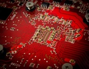
With the never-ending drive for smaller, lighter and more advanced features on portable products, the ability to handle miniaturization is becoming a key capability to enable these requirements. Miniaturization can be done in many ways and this article touches on the assembly technologies that can be incorporated in a more or less standard surface mount assembly line with minimal equipment and material upgrades.
Before starting any development work it is critical to understand product and industry requirements and capabilities. If this is not fully understood, no development activities can start. PCB fabrication can be seen as a good example on the importance of understanding requirements and capabilities. If a good quality PCB can’t be sourced within the scope of the assembly development project there is no reason to develop an assembly technology process since there is not anything to do the assembly development work on. The key is to ensure that several options for assembly can be achieved and this should be seen as a toolbox of technologies.
For the active components die stacking inside a package is one common way to increase the functionality per unit area on a PCBA, which is very popular for memory devices. However, there can be some drawbacks to creating a stacked die solution. First, this method is a customized solution. If any of the dies to be used changes, the die stack needs to be evaluated to see if changes are needed in the package. For example, a die shrink may occur and this could change the whole package structure. Secondly, if one or more of the dies inside the package fail, the whole unit will have to be scrapped, which would lead to increased cost; this is the well-known compounded yield issue. Lastly, trying to coordinate the many semiconductor suppliers to provide dies to a packaging house for die stacking can be a challenging task and overall responsibility for the complete package yield could in some cases be unclear.
In the PoP process one component is placed on top of another package during a single SMT process to fully utilize the three dimensional aspect of the product. The topside of the bottom component has pads similar to the pads on the PCB for attachment of the top package. Each package is a single unit that can be fully tested as a normal IC package is done today, so the yield would be comparable to the normal yield commonly seen today. Another advantage would be the ability to have second-source options that could be fairly easily inserted into the process.
The stacked package can be processed in a traditional SMT environment with a few upgrades that are readily available. Therefore, package stacking enables configurable assemblies and provides greater flexibility in the supply chain. It can be used for memory applications or for a processor with memory, with faster time to market and better management of package testing and compounded yield issues.
Editor's Note: This article originally appeared in the May 2015 issue of SMT Magazine.
Share on:


Suggested Items
Determining the Value-add of Box Build
04/24/2024 | Nolan Johnson, I-Connect007At a strategic level, adding box-building services makes sense for customer loyalty. But is it really that simple? Jon Schmitz, who manages customer engagement at RiverSide Integrated Solutions, talk about about what it really takes to be successful in offering EMS and final assembly services under the same company banner.
IMAPS & IPC to Host Onshoring Workshop
04/16/2024 | IPCThe International Microelectronics Assembly and Packaging Society (IMAPS) and IPC will host an Onshoring Workshop to discuss ongoing progress and forward-looking strategies to drive the Onshoring Advanced Packaging and Assembly, April 29 – May 1, 2024, in Arlington, Virginia.
IPC WinterCom 2024 Through the Eyes of One Dedicated Student
04/12/2024 | Sanjay Huprikar, IPCLauriane Testuz stands as a testament to the power of curiosity, perseverance, and the relentless pursuit of knowledge. Her story serves as a reminder that the path to success is often paved by an unwavering commitment to one's dreams.
2023: Year of Extremes for VDL Groep
04/08/2024 | VDL GroepThe year 2023 showed us two sides, with highs and lows. Low points were the passing of Wim van der Leegte in November, the reduction in the number of employees at VDL Nedcar and headwind in the Buses & Coaches division.
IPC, First and Only Organization in the Electronics Industry to Earn ANSI/ANAB Accreditation for Its Workforce Training
04/02/2024 | IPCIPC, the global leader in electronics education, announces a landmark achievement in professional education and training. Ten of IPC’s critical workforce training programs have been accredited by the ANSI National Accreditation Board (ANAB) under the stringent requirements of ANSI/ASTM E2659-18, Standard Practice for Certificate Programs.