


 Global Sourcing Spotlight: The Hidden Power of the Rep Network
 Smart Automation: When Traditional Depaneling Methods Reach Their Limits
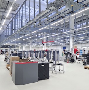
 Powering the Future: When Material Choice Defines RF Performance


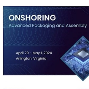
The International Microelectronics Assembly and Packaging Society (IMAPS) and IPC will host an Onshoring Workshop to discuss ongoing progress and forward-looking strategies to drive the Onshoring Advanced Packaging and Assembly, April 29 – May 1, 2024, in Arlington, Virginia.
This workshop will bring together Government agencies, the DIB (Defense Industrial Base) and Advanced Packaging and Assembly stakeholders to discuss their ongoing efforts to develop advanced packaging capability onshore. The mission of this event is to engage the domestic semiconductor industry by providing updates on US Government and Defense initiatives that are critical to the onshoring of the microelectronic assembly and packaging supply chain. Advanced packaging initiatives lead by numerous Government agencies, including the Department of Commerce/NIST (ME Commons, NAPMP and NSTC), DoD (RESHAPE, SHIP, STAM, STEAM PIPE, SCALE, IBAS, Title III), and DARPA (NGMM) will be presenting.
The workshop will feature three days of program focused sessions, informative keynote presentations, a work force development session, panel discussions and a variety of networking opportunities. The event will kick-off on Monday April 29th with a pre-program day with 2-hour professional development courses and/or additional working groups addressing a variety of topics relevant to the onshoring of advanced packaging. The 2024 workshop also features opportunities for sponsorship and tabletop exhibitors.
Attendees can help shape another successful Onshoring Workshop by contributing their valuable insight! A United States Passport is required for registration.
Keynotes include:
- Ms. Adele Ratcliff, Director of Innovation Capability and Modernization (ICAM) Office
- Dr. Dev Palmer, Next-Generation Microelectronics Manufacturing (NGMM) Program Managing Director, DARPA
- Dr. Dev Shenoy, Office of the Undersecretary of Defense, Director of the Defense Microelectronics Cross Functional Team
- Dr. Eric Lin, Deputy Director, CHIPS Research and Development Program
- Dr. George Orji, Deputy Director, Chips NAPMP
- Dr. Joshua Hawke, Navy, OUSD R&E RF/OE Initiatives, Technical Execution Area Lead
- Ms. Molly Just, Director of CHIPS Coordination Cell, OUSD A&S
Comment from the Technical Program Chair:
“With the exceptional engagement of our Technical Steering Committee members, we have assembled a comprehensive program for this year’s Workshop with representation from all of the US Government and Defense agencies that are tasked with driving the advanced packaging onshoring efforts and associated supply chain stakeholder enhancements. During this event, attendees will be updated directly from DoD leaders and their industry performers on current and future programs that will address and inform U.S. Government advanced packaging roadmaps. This workshop also provides outstanding opportunities to interface with multiple levels of Government leadership, the Defense Industrial Base, and Commercial Suppliers, all of whom share a common goal to make the USA more self-sufficient in microelectronics manufacturing.” ~ Ted Tessier, IBM


