


 Standard of Excellence: Speed vs. Quality in Customer Service
 Knocking Down the Bone Pile: Revamp Your Components with BGA Reballing
 Global Sourcing Spotlight: Balancing Speed and Flexibility Without Sacrificing Control


ESI's Most Extensible Laser Micromachining Platform Delivers Efficient Manufacturing for Consumer Electronics
June 25, 2015 | ESIEstimated reading time: 2 minutes
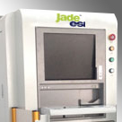
Electro Scientific Industries, Inc., an innovator of laser-based manufacturing solutions for the micromachining industry, today introduced Jade™, the new low-cost, high-volume-production laser micromachining platform adaptable to a range of configurations for different applications including cutting, marking, drilling and engraving.
The new platform addresses challenges faced by manufacturers in the fast-changing consumer electronics segment where they cope with new materials, new technologies and evolving consumer expectations. Meanwhile, there is relentless pressure to reduce costs, meet quality requirements and achieve high-volume high-yield production. The Jade™ platform is the first laser micromachining platform capable of meeting all these diverse requirements, offering unprecedented levels of versatility and cost-efficient operation.
"Production requirements in consumer electronics are constantly changing with new materials and features that require a range of laser micromachining processes that can be delivered quickly and at an attractive cost of ownership," said Edward C. Grady, President and CEO of ESI. "We are directly addressing this challenge with the Jade™ platform. Designed by ESI's cooperative China-USA engineering operation, this low-cost platform is adaptable, reliable, and locally built and serviced by our support teams on the ground in China."
The Jade™ platform is designed to provide contract and consumer electronics manufacturers with a smarter manufacturing option through the use of extendable and configurable stages, lasers, and automation. The base platform can be configured with multiple laser and optics options as well as a range of add-on options including pre- and post-inspection, metrology and advanced alignment automation. All configurations use a common user interface to reduce training time.
This flexibility means that a Jade™ platform can address multiple marking, cutting, and drilling applications in a responsive and cost-effective manner, improving the useful lifespan of the tool and significantly lowering overall cost of ownership for our customers. The Jade™ platform continues ESI's commitment to reliability, responsive local support in China, and to meeting expectations for precision and high-volume yields.
Availability
The Jade™ Series of platforms are available now in China, Vietnam, India, Korea and Taiwan. For more information go to www.esi.com.
About ESI
ESI's integrated solutions allow industrial designers and process engineers to control the power of laser light to transform materials in ways that differentiate their consumer electronics, wearable devices, semiconductor circuits and high-precision components for market advantage. ESI's laser-based manufacturing solutions feature the micro-machining industry's highest precision and speed, and target the lowest total cost of ownership. ESI is headquartered in Portland, Ore., with global operations from the Pacific Northwest to the Pacific Rim. More information is available at www.esi.com.
Share on:


Testimonial
"Our marketing partnership with I-Connect007 is already delivering. Just a day after our press release went live, we received a direct inquiry about our updated products!"
Rachael Temple - AlltematedSuggested Items
Henger Microelectronics Expands Global Footprint with Major Equipment Shipment to Southeast Asia
10/31/2025 |Henger Microelectronics has reached a major milestone in its global expansion strategy with the successful shipment of advanced plasma etching and cleaning systems, along with automation equipment, to multiple countries and regions across Southeast Asia. This achievement marks a significant step forward in the company’s international growth and reinforces its position as a leading force in the global plasma equipment industry.
TTCI Brings Hands-On Test Engineering and IPC Training Expertise to PCB Carolina 2025
10/31/2025 | The Test Connection Inc.The Test Connection Inc. (TTCI), a trusted provider of electronic test and manufacturing solutions, and The Training Connection LLC (TTC-LLC) will exhibit at PCB Carolina on Wednesday, November 12, 2025, at the McKimmon Center at NC State University in Raleigh, North Carolina. Attendees can visit Table 4 to say hello to Bert Horner and Bill Graver, and learn more about their test engineering services and technical training programs.
Cephia Secures $4M Seed Funding to Revolutionize Multimodal Sensing with Metasurface Technology
10/31/2025 | PRNewswireCephia, a startup building products using advanced AI computational imaging technologies and silicon sensors made from advanced metamaterials, formally launched with several pilot customers and $4 million in seed venture capital funding.
I-Connect007 Editor’s Choice: Five Must-Reads for the Week
10/31/2025 | Nolan Johnson, I-Connect007Last week, the IMPACT conference took place in Taipei, bringing together advanced packaging experts from around the globe to share their knowledge. We’ll be bringing you post-conference coverage over the next few weeks, so look for that in our newsletters, and in the Advanced Electronic Packaging Digest. Other news seemed to have the U.S. at the center of the global discussions. My picks start in Phoenix, where TSMC, NVIDIA, and Amkor are all scrambling to establish new capabilities. There’s nothing like a strong demand signal to cause build-out, and AI chips are doing exactly that.
NEDME 2025 Draws Strong Northwest Crowd, Builds on Tradition of Regional Collaboration
10/31/2025 | NEDMEThe NW Electronics Design & Manufacturing Expo (NEDME) 2025 once again brought together the Pacific Northwest community for a full day of learning, networking, and industry connections.