


 Punching Out: How Are the Big Boys in Electronics Doing?
 It’s Only Common Sense: Complexity Is the Enemy of Profit
 Dan’s Biz Bookshelf: ‘Abundance: How We Build a Better Future’


Ventec to Focus on ‘tec-speed’ Brand for High Speed/Low Loss Materials at IPC APEX 2016
March 8, 2016 | Ventec International GroupEstimated reading time: 2 minutes
Ventec International Group, a world leader in the production of polyimide and high-reliability epoxy laminates and prepregs, unveiled their high-speed/low-loss product portfolio, tec-speed, in January 2016. Ventec will be showcasing the range globally at a number of shows this year. Starting with IPC APEX EXPO in Las Vegas (15-17 March 2016), tec-speed will be a highlight at Ventec’s booth number 827 with an emphasis on the mil/aero applications.
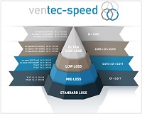
Tec-speed unites Ventec's high-speed/low-loss product portfolio and better positions the range under a single identity, connecting the products through a clear and cohesive visual presentation. The tec-speed laminates and prepregs range from mid-loss (Df 0.012) to ultra-low-loss (Df 0.003) specifications with Dk levels ranging between 3.9 and 3.2, offering the ultimate in laminate technology and quality assurance through Ventec's proprietary manufacturing and distribution network.
Jack Pattie, president of Ventec USA, said, “Thermal performance and signal integrity demands are increasing, particularly for mil/aero applications where miniaturization and density of components are pushing the boundaries of PCB design. Tec-speed materials and our strategic roadmap of new innovative additions to the range, provide the technological innovation, high performance and quality demanded by our customers.”
A selection of products will be highlighted at the show, including:
- tec-speed 6.1 (Dk 3.2, Df 0.004 RC 50%) - Ultra-Low Loss High-Tg material available with all copper styles, including HVLP. Uses low Dk spread glass to improve skew and jitter. Applications include telecom, router, servers, etc. Specifically developed for backplane and daughter card designs where good signal integrity is essential. This material has excellent thermal properties.
- tec-speed 4.0 (Dk 3.8, Df 0.007) - Low-loss high-Tg material available with all copper styles, including HVLP. Applications focus on high-frequency and high-speed designs, Automotive and satellite communication, Navigation and GPS are typical applications. This material has excellent thermal properties.
- tec-speed 1.0 (Dk 3.9, Df 0.012 @ 10GHz RC75%) - Mid-loss mid-Tg halogen-free material available with all copper styles. Applications include hand-held products, specifically those that require high-frequency high-speed materials. This material has excellent thermal properties.
About Ventec International
With volume manufacturing facilities and HQ in Suzhou China, Ventec International specializes in advanced copper clad glass reinforced and metal backed substrates for the PCB industry. With distribution locations and quick-turn CCL manufacturing sites in both the US and Europe, Ventec International is a premier supplier to the Global PCB industry. For more information about Ventec’s solutions and the company’s wide variety of products, please click here or download to the Ventec APP.
Share on:


Testimonial
"Advertising in PCB007 Magazine has been a great way to showcase our bare board testers to the right audience. The I-Connect007 team makes the process smooth and professional. We’re proud to be featured in such a trusted publication."
Klaus Koziol - atgSuggested Items
I-Connect007 Releases The Printed Circuit Designer’s Guide to… Direct Metallization: A Guide to Complex PCB Fabrication
05/12/2026 | I-Connect007As PCB complexity continues to accelerate, fabricators and OEMs are reevaluating long-standing manufacturing processes to meet the demands of AI, HDI, advanced packaging, and next-generation electronics. To address these evolving challenges, I-Connect007 is proud to announce the release of The Printed Circuit Designer’s Guide to… Direct Metallization: A Guide to Complex PCB Fabrication, authored by MacDermid Alpha Solution’s Carmichael Gugliotti.
Driving Innovation: Selecting the Right Laser Source
04/28/2026 | Simon Khesin -- Column: Driving InnovationWhen I first joined Schmoll Maschinen, I brought experience from almost every PCB process, except for laser. As I immersed myself in laser processing, I realized why it can seem so daunting to a newcomer. The complexity arises from three intersecting factors: A vast variety of laser sources: CO2, UV-nano, green-pico, UV-pico, IR-pico, and others; a diverse range of applications: Drilling, cutting, ablation, and more; and an extensive list of materials: These have vastly different absorption rates. Choosing the right machine or laser source is rarely trivial. Even for experienced engineers, answering "Which source is best?" requires examining the business's specific goals.
Institute of Circuit Technology Spring Seminar 2026: A Bright Future in Europe
04/23/2026 | Pete Starkey, I-Connect007Through the leafy lanes and spring flowers of Warwickshire and back to Meridan, the traditional centre of England, and now officially part of the Metropolitan Borough of Solihull in the county of the West Midlands, I attended the Annual General Meeting and Spring Seminar of the Institute of Circuit Technology (ICT) on April 14. Out of the AGM came notable changes in leadership at the top of the Institute: the retirement of Mat Beadel as chair and Emma Hudson as technical director. Effective May 1, Steve Driver is the new chair, and Alun Morgan is the new technical director.
ACCM Unveils Negative and Near-zero CTE Materials for Large-Format AI Chips
04/21/2026 | Advanced Chip and Circuit MaterialsAdvanced Chip and Circuit Materials, Inc. (ACCM) has launched two new materials: Celeritas HM50, with a negative coefficient of thermal expansion (CTE) of -8 ppm/°C to offset the positive CTE and expansion of copper with temperature on circuit boards, and Celeritas HM001, with near-zero CTE and the low-loss performance needed for high-speed signal layers to 224 Gb/s and faster in artificial intelligence (AI) circuits.
Fresh PCB Concepts: Designing PCBs for Harsh Environments—Reliability Is Engineered Upstream
04/23/2026 | Team NCAB -- Column: Fresh PCB ConceptsWhen engineers hear the phrase “harsh environment,” they usually think of the extreme temperature swings, vibration and shock, pressure changes, or radiation in aerospace. However, aerospace is not the only harsh environment where electronic assemblies must survive. Automotive power electronics, downhole oil and gas tools, marine controls, rail systems, defense platforms, and industrial automation equipment all expose PCBs to environments that are equally unforgiving. The stress mechanisms may differ, but the physics does not.