


 Beyond Design: The Fundamental Structure of Spectral Integrity
 Elementary, Mr. Watson: High Power: When Physics Becomes Real
 The Shaughnessy Report: Watt About Power Integrity?


The Importance of Design for Profit (DFP)
July 5, 2016 | Barry Matties, I-Connect007Estimated reading time: 1 minute
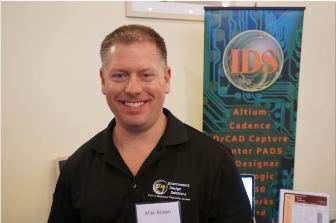
In this interview, Interconnect Design Solutions’ Mike Brown and I took a few minutes during the recent Geek-A-Palooza event to discuss the importance of material selection and designing for profitability, how automation affects the design process, and the future of the design community.
Barry Matties: Mike, tell me a little bit about IDS and what you do.
Mike Brown: We provide PCB layout and mechanical engineering services as an extension for OEMs as well as bareboard fabricators and assemblers that need design support. Basically, we're in the trenches working with the electrical engineers to help realize our product and bring it to market.
Matties: Are you doing actual design for customers or are you just assisting and educating?
Brown: We're actually doing design at the rigid board level, the flex-rigid, and flex board level as well as mechanical engineering and enclosure design. We're helping engineers realize their project from concept through reality.
Matties: So you start from the beginning?
Brown: We start from the beginning with a functional spec. We're sitting there basically looking at a block diagram sometimes.
Matties: It's a collaborative effort?
Brown: Yes, it is very collaborative.
Matties: Isn't that the best way to go, really?
Brown: It is. You have to be engaged in the beginning in order to be successful in the end.
Matties: And yet many engineers don't take this track; what’s the downside of that?
Brown: The problem is there's a lack of communication and in a lot of cases, multiple spins of your product can occur; which in turn costs more because you typically don't have your pwb layout designer collaborating up front with your primary engineering team. The layout designer really needs to understand the product from the beginning. They need to understand the design intent and what the end goal of the product is. By having them involved in the beginning up front at the functional spec level and then at the detail spec level, they can help make conscious decisions that ultimately will affect the overall cost, time line and schedule of the product.
To read this entire article, which appeared in the June 2016 issue of The PCB Design Magazine, click here.
Share on:


Testimonial
"In a year when every marketing dollar mattered, I chose to keep I-Connect007 in our 2025 plan. Their commitment to high-quality, insightful content aligns with Koh Young’s values and helps readers navigate a changing industry. "
Brent Fischthal - Koh YoungSuggested Items
Peters, Starteam, and Würth Elektronik Team Up For Digital Coating Technology
10/23/2025 | PetersUnder this heading, the PCB manufacturers Starteam and Würth Elektronik, along with Peters as inkjet coating supplier, have taken the initiative and worked together for months in trusting and target-oriented cooperation, to promote this innovative digital coating technology for solder resists and establish it on the market.
AI Triggers Next Paradigm Shift in PDN
10/23/2025 | Istvan Novak, SamtecArtificial intelligence (AI), together with machine learning (ML), is creating an unprecedented surge of computing and networking infrastructure needs. This, in turn, has dramatically increased the power consumption of computing and networking chips.
SEMICON Japan 2025 to Spotlight Sustainability in AI and Semiconductor Innovation
10/22/2025 | SEMISEMICON Japan 2025, the largest gathering of leaders from the microelectronics manufacturing supply chain in Japan, will bring together more than 1,200 exhibitors showcasing semiconductor solutions from December 17-19 at Tokyo Big Sight.
Zuken Announces ZIW Americas 2026 in Dallas
10/21/2025 | ZukenZuken USA, Inc., a global leader in electrical and electronic design automation, announced Zuken Innovation World (ZIW) Americas 2026, the company’s premier global conference dedicated to advancing the future of electrical and electronic product design. ZIW 2026 will be held June 9-11 in Dallas, Texas.
Keysight Completes Acquisition of Synopsys’ Optical Solutions Group and Ansys’ PowerArtist
10/17/2025 | Keysight Technologies, Inc.Keysight Technologies, Inc., announced the completion of its acquisitions of the Optical Solutions Group from Synopsys, Inc., and PowerArtist from Ansys, Inc.