-
- News
- Books
Featured Books
- design007 Magazine
Latest Issues
Current IssueProper Floor Planning
Floor planning decisions can make or break performance, manufacturability, and timelines. This month’s contributors weigh in with their best practices for proper floor planning and specific strategies to get it right.
Showing Some Constraint
A strong design constraint strategy carefully balances a wide range of electrical and manufacturing trade-offs. This month, we explore the key requirements, common challenges, and best practices behind building an effective constraint strategy.
All About That Route
Most designers favor manual routing, but today's interactive autorouters may be changing designers' minds by allowing users more direct control. In this issue, our expert contributors discuss a variety of manual and autorouting strategies.
- Articles
- Columns
- Links
- Media kit
||| MENU - design007 Magazine
Mentor Graphics Video: Concurrency During Schematic Design
January 3, 2017 | Mentor GraphicsEstimated reading time: Less than a minute

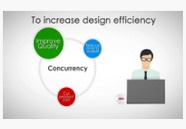
Increasing design efficiency is the biggest challenge in the PCB business today.
Design teams are pushed to continually add product functionality while reducing design time, cutting product costs, and improving product quality. A recent survey by Aberdeen identifies increased pressure to meet delivery deadlines as the number one driver of improvements in PCB processes.
The answer to this challenge is concurrent team work throughout the entire design flow.
Watch this video and learn how to reduce design time, cut product costs, and improve product quality by enabling PCB engineering teams to collaborate in real-time with concurrent schematic design technology.
Testimonial
"Our marketing partnership with I-Connect007 is already delivering. Just a day after our press release went live, we received a direct inquiry about our updated products!"
Rachael Temple - AlltematedSuggested Items
Global PCB Connections: Understanding the General Fabrication Process—A Designer’s Hidden Advantage
08/14/2025 | Markus Voeltz -- Column: Global PCB ConnectionsDesigners don’t need to become fabricators, but understanding the basics of PCB fabrication can save you time, money, and frustration. The more you understand what’s happening on the shop floor, the better you’ll be able to prevent downstream issues. As you move into more advanced designs like HDI, flex circuits, stacked vias, and embedded components, this foundational knowledge becomes even more critical. Remember: the fabricator is your partner.
The Art and Science of PCB Floor Planning: A Comprehensive Guide
08/14/2025 | Cory Grunwald and Jeff Reinhold, Monsoon SolutionsPCB design is an intricate and crucial part of developing electronic products. One of the foundational stages of PCB design is floor planning, a phase where the placement of components and the flow of signals are meticulously mapped out. A good floor plan ensures that the PCB performs well, is easy to manufacture, and meets all mechanical and electrical requirements. We’ll explore the essential aspects of floor planning, from its objectives and process to the challenges that designers face.
EnSilica Establishes New EU Mixed-Signal Design Centre in Budapest, Hungary
08/12/2025 | EnSilicaThe facility strengthens EnSilica’s presence in the European Union and taps into Budapest’s deep technology ecosystem, which hosts numerous leading automotive and industrial multinationals. This expansion will increase the Group’s global headcount to around 210 employees.
Happy’s Tech Talk #41: Sustainability and Circularity for Electronics Manufacturing
08/13/2025 | Happy Holden -- Column: Happy’s Tech TalkI attended INEMI’s June 12 online seminar, “Sustainable Electronics Tech Topic Series: PCBs and Sustainability.” Dr. Maarten Cauwe of imec spoke on “Life Cycle Inventory (LCI) Models for Assessing and Improving the Environmental Impact of PCB Assemblies,” and Jack Herring of Jiva Materials Ltd. spoke on “Transforming Electronics with Recyclable PCB Technology.” This column will review information and provide analysis from both presentations.
Elementary, Mr. Watson: Why Your PCB Looks Like a Studio Apartment
08/13/2025 | John Watson -- Column: Elementary, Mr. WatsonIn November 2022, I wrote a column called "Is Your Bathroom in the Kitchen?" This piece related a bizarre real estate listing that emerged out of St. Louis that had architects scratching their heads and interior designers cringing. Nestled in the historic Central West End sat a 200-square-foot apartment that completely defied logic. It wasn't the size that raised eyebrows, it was the layout. Here's the kicker: While that's rare in real estate, it's shockingly common in PCB design.