-
- News
- Books
Featured Books
- smt007 Magazine
Latest Issues
Current IssueIntelligent Test and Inspection
Are you ready to explore the cutting-edge advancements shaping the electronics manufacturing industry? The May 2025 issue of SMT007 Magazine is packed with insights, innovations, and expert perspectives that you won’t want to miss.
Do You Have X-ray Vision?
Has X-ray’s time finally come in electronics manufacturing? Join us in this issue of SMT007 Magazine, where we answer this question and others to bring more efficiency to your bottom line.
IPC APEX EXPO 2025: A Preview
It’s that time again. If you’re going to Anaheim for IPC APEX EXPO 2025, we’ll see you there. In the meantime, consider this issue of SMT007 Magazine to be your golden ticket to planning the show.
- Articles
- Columns
Search Console
- Links
- Media kit
||| MENU - smt007 Magazine
KIC to Feature SPS Smart Profiler at SMTA Ohio Expo & Tech Forum
June 13, 2017 | KICEstimated reading time: 1 minute

KIC plans to exhibit at the SMTA Ohio Expo & Tech Forum, scheduled for Thursday, July 13, 2017 at the Embassy Suites Cleveland Rockside in Independence (Cleveland), Ohio. MB (Marybeth) Allen will showcase discuss how to turn your factory into a Smart Factory with KIC’s new SPS Smart Profiler reflow process inspection tool and all new KIC Vantage network insight software.
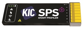
The core function of a reflow oven is to produce an acceptable profile on each PCB. The new KIC SPS smart profiler collects the profile data and compares it to the process specifications. Within seconds, the new smart profiler also suggests an improved reflow oven setup. The thermal profiler features a small compact design made with an LCP (Liquid Crystal Polymer) enclosure for better heat protection and faster cool-down between profiles.
The KIC Vantage network intelligence system is an ecosystem that automatically acquires and delivers insightful information from all the ovens in the factory in real-time to allow factories to produce consistent quality at lower costs. The software is retrofitable and can connect to the factory MES system.
About KIC
Based in San Diego, KIC is the industry leader in automated thermal process tools and systems for reflow, wave, curing and semiconductor thermal processes. The company pioneered the development of oven profilers and process optimization tools, and then worked to create the next generation of thermal systems to help manufacturers improve the thermal process quality while reducing cost.
KIC products include the KIC SPS, K2, X5, KICstart2, ProBot, 24/7 Wave and the KIC RPI. With the introduction of cutting edge tools, the company continues to stay on the leading edge of process optimization and automatic thermal process systems, and has won numerous industry awards.
For more information about KIC, click here.
Suggested Items
Scanfil Boosts Investment in Electronics Manufacturing in the US
05/08/2025 | BUSINESS WIREScanfil is investing in a second electronics manufacturing line in Atlanta, Georgia, USA. The demand for manufacturing electronics in the USA has increased over the past two years and is expected to continue growing.
ZESTRON Announces New Reliability and Solutions Service for Risk Assessment & Mitigation of Electronic Assemblies
05/06/2025 | ZESTRONZESTRON, the leading global provider of high-precision cleaning products, services, and training solutions, is thrilled to introduce its new Reliability and Solutions (R&S) service.
Trouble in Your Tank: Causes of Plating Voids, Pre-electroless Copper
05/09/2025 | Michael Carano -- Column: Trouble in Your TankIn the business of printed circuit fabrication, yield-reducing and costly defects can easily catch even the most seasoned engineers and production personnel off guard. In this month’s column, I’ll investigate copper plating voids with their genesis in the pre-plating process steps.
Knocking Down the Bone Pile: Gold Mitigation for Class 2 Electronics
05/07/2025 | Nash Bell -- Column: Knocking Down the Bone PileIn electronic assemblies, the integrity of connections between components is paramount for ensuring reliability and performance. Gold embrittlement and dissolution are two critical phenomena that can compromise this integrity. Gold embrittlement occurs when gold diffuses into solder joints or alloys, resulting in mechanical brittleness and an increased susceptibility to cracking. Conversely, gold dissolution involves the melting away of gold into solder or metal matrices, potentially altering the electrical and mechanical properties of the joint.
Happy’s Tech Talk #38: Novel Metallization for UHDI
05/07/2025 | Happy Holden -- Column: Happy’s Tech TalkI have been involved in high-density electronics substrates since 1970 when I joined Hewlett-Packard’s RF semiconductor group after college. Figure 1 shows the difference between trace/space lithography for substrates and silicon starting in 1970. My projects involved sapphire circuits for RF devices, but the figure displays the state of PCBs and integrated CMOS circuits and their packaging, not discreet RF devices. Even then, semiconductors were 50X higher density.