-

- News
- Books
Featured Books
- design007 Magazine
Latest Issues
Current Issue
Signal Integrity
If you don’t have signal integrity problems now, you will eventually. This month, our expert contributors share a variety of SI techniques that can help designers avoid ground bounce, crosstalk, parasitic issues, and much more.

Proper Floor Planning
Floor planning decisions can make or break performance, manufacturability, and timelines. This month’s contributors weigh in with their best practices for proper floor planning and specific strategies to get it right.

Showing Some Constraint
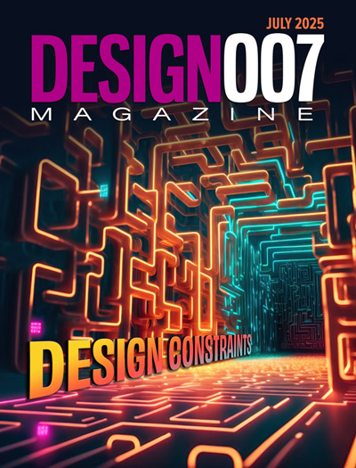
A strong design constraint strategy carefully balances a wide range of electrical and manufacturing trade-offs. This month, we explore the key requirements, common challenges, and best practices behind building an effective constraint strategy.
- Articles
- Columns
- Links
- Media kit
||| MENU - design007 Magazine
It’s Not Your Father’s DFM Anymore
September 28, 2017 | Pat McGoff, MentorEstimated reading time: 1 minute
Trivia question for you: What was the first design for manufacturing (DFM) tool used in the PCB industry? Answer: The eye loop.
Yes, back in the day when design organizations sent actual photoplotted films of their PCB design to the bareboard fabricator, the fabricator would put the received films on a light table and measure feature sizes for line widths, spacing between features and annular ring using an eye loop with a reticle etched onto the glass lens. If the features were beyond the capabilities of the fabricator, the job would be declined and the customer notified. If the film had extraneous features they would be removed with an Exacto knife. Voids would be filled in using a black marker.
Simpler times, then. Ten mil lines and spaces and double-sided PCBs were the norm. Manual DFM was feasible.
Needless to say, our industry has advanced in technology since those days. We have PCBs that exceed 64 layers, build-up technology with laser-formed stacked and staggered microvias, embedded devices, and complex rigid-flex circuits. And our design, fabrication, and assembly processes morphed into the new global economy, and in many cases, outsourced and off-shored.
So, what does DFM look like today? Well, for one, it’s become more than DFM. We now expect our software tools to serve us more completely to take new designs to market. DFM has evolved to become an integral part of new product introductions (NPI). Today’s NPI software spans design and manufacturing to accelerate the optimization of a PCB for manufacturing. It looks at the entire design-to-manufacturing release process and deliverables, then streamlines them.
Engineers at best-practice companies use NPI software to help identify ways to optimize their design during the initial release process, with a holistic view of their bareboard fabricators’ and assembly suppliers’ capabilities. It’s not simply a matter of catching mistakes these days. It’s about understanding the various challenges and limitations involved in the chosen manufacturing processes and then empowering the product owner to make the trade-off decisions that best serve their objectives.
To read this entire article, which appeared in the September 2017 issue of The PCB Design Magazine, click here.
Testimonial
"We’re proud to call I-Connect007 a trusted partner. Their innovative approach and industry insight made our podcast collaboration a success by connecting us with the right audience and delivering real results."
Julia McCaffrey - NCAB GroupSuggested Items
Siemens, TRUMPF Partner to Accelerate Digital Manufacturing and AI Readiness
09/16/2025 | SiemensTechnology company Siemens and leading machine tools and laser manufacturer TRUMPF announced a partnership that promises to elevate industrial production by harnessing advanced digital manufacturing solutions.
I-Connect007 Launches Advanced Electronics Packaging Digest
09/15/2025 | I-Connect007I-Connect007 is pleased to announce the launch of Advanced Electronics Packaging Digest (AEPD), a new monthly digital newsletter dedicated to one of the most critical and rapidly evolving areas of electronics manufacturing: advanced packaging at the interconnect level.
ICAPE Group Unveils Exclusive Report on Sustainability in Electronics Manufacturing
09/15/2025 | ICAPE GroupICAPE Group, a global leader in printed circuit boards (PCBs) and custom electronics manufacturing, today announces the launch of its 2025 Industry Outlook & Innovation Report: Sustainability in Electronics Manufacturing. This exclusive report is accompanied by fresh insights from a dedicated Statista survey of 100 electronics manufacturing professionals, commissioned by ICAPE Group.
Panasonic Industry will Double the Production Capacity of MEGTRON Multi-layer Circuit Board Materials Over the Next Five Years
09/15/2025 | Panasonic Industry Co., Ltd.Panasonic Industry Co., Ltd., a Panasonic Group company, announced plans for a major expansion of its global production capacity for MEGTRON multi-layer circuit board materials today. The company plans to double its production over the next five years to meet growing demand in the AI server and ICT infrastructure markets.
Sustainability and Selective Soldering
09/15/2025 | Dr. Samuel J. McMaster, Pillarhouse InternationalSustainability is more than just a buzzword for the electronics industry; it’s a key goal for all manufacturing processes. This is more than a box-ticking exercise or simply doing a small part for environmentally friendly processes. Moving toward sustainable solutions drives innovation and operational efficiency.


