-

- News
- Books
Featured Books
- design007 Magazine
Latest Issues
Current Issue
Signal Integrity
If you don’t have signal integrity problems now, you will eventually. This month, our expert contributors share a variety of SI techniques that can help designers avoid ground bounce, crosstalk, parasitic issues, and much more.

Proper Floor Planning
Floor planning decisions can make or break performance, manufacturability, and timelines. This month’s contributors weigh in with their best practices for proper floor planning and specific strategies to get it right.

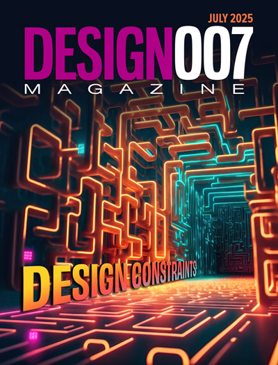
Showing Some Constraint
A strong design constraint strategy carefully balances a wide range of electrical and manufacturing trade-offs. This month, we explore the key requirements, common challenges, and best practices behind building an effective constraint strategy.
- Articles
- Columns
- Links
- Media kit
||| MENU - design007 Magazine
The History of Predictive Engineering
November 1, 2017 | Happy Holden, I-Connect007Estimated reading time: 2 minutes
It all started in 1983, at HP, when I complained to our group's vice president that our W. Edwards Deming and Total Quality Management (TQM) Six Sigma training was being concentrated in PCB manufacturing. We had eliminated final inspection and instead placed quality in the hands of the operators with a final electrical test. The electrical test was governed by what we learned from Deming.
Our customers’ problems with on-time delivery and rejects had gone away, but now our problem was that we were having to put all our engineering at the front end of the process to inspect incoming CAD designs for producibility, as the PCB design groups had no concept of a “quality design.” To them their customer was the electronic designer and the schedule. To meet the schedules, they would just throw the design “over the wall,” even though they knew the designs had problems.
“Since you understand the problem, I am going to promote you to PCB design services manager,” said the VP, agreeing with me. “In integrated circuits, we design the physical chips and then fabricate them from the specs and circuits the EE gives us. I have never understood why the PCB fab group also did not do PCB layout in the IC model!”
Not the answer I wanted, but at least he gave me the budget and the designers’ salary flexibility I needed to recruit and start a PCB layout group as part of PCB manufacturing. So, DFM became the central focus for our design strategy.
DFM/A was just starting out at HP. HP had taken a license from Hitachi and GE to use the Dewhurst and Boothroyd DFM/A methodology. This came after extensive benchmarking review of past HP product designs and visiting other large manufacturing companies like John Deere, Ford, Hitachi, Caterpillar, and Western Electric. The benchmarking clearly showed that just hiring the smartest engineers and giving them the best EDA tools did not guarantee a superior product. The electronic circuits may have been superior, but the physical products were far too overdesigned’ and complex, thus adding a lot of unnecessary costs and complexity.
The D&B DFM/A methodology was used concurrently with the physical design to point out complexities and provided feedback on how to simplify. It was also used to benchmark competitor’s products. The DFM/A methodology was focused on “Doing it right the first time.” This was not a design rule checker, and a lot more useful than “best practices,” although these are useful tools. This is where I get my definition of DFM or DFX.
CAM software, including DRCs, are activities that take place after the design is finished. We found one EDA supplier, Zuken, that had “design advisor” software for signal integrity, which they gained when they acquired Racal-Redac. This software resided on the screen and provided real-time feedback on SI as they routed traces by taking variables from the database and doing a real-time simulation.
To read this entire article, which appeared in the September 2017 issue of The PCB Design Magazine, click here.
Testimonial
"Advertising in PCB007 Magazine has been a great way to showcase our bare board testers to the right audience. The I-Connect007 team makes the process smooth and professional. We’re proud to be featured in such a trusted publication."
Klaus Koziol - atgSuggested Items
Siemens, TRUMPF Partner to Accelerate Digital Manufacturing and AI Readiness
09/16/2025 | SiemensTechnology company Siemens and leading machine tools and laser manufacturer TRUMPF announced a partnership that promises to elevate industrial production by harnessing advanced digital manufacturing solutions.
I-Connect007 Launches Advanced Electronics Packaging Digest
09/15/2025 | I-Connect007I-Connect007 is pleased to announce the launch of Advanced Electronics Packaging Digest (AEPD), a new monthly digital newsletter dedicated to one of the most critical and rapidly evolving areas of electronics manufacturing: advanced packaging at the interconnect level.
ICAPE Group Unveils Exclusive Report on Sustainability in Electronics Manufacturing
09/15/2025 | ICAPE GroupICAPE Group, a global leader in printed circuit boards (PCBs) and custom electronics manufacturing, today announces the launch of its 2025 Industry Outlook & Innovation Report: Sustainability in Electronics Manufacturing. This exclusive report is accompanied by fresh insights from a dedicated Statista survey of 100 electronics manufacturing professionals, commissioned by ICAPE Group.
Panasonic Industry will Double the Production Capacity of MEGTRON Multi-layer Circuit Board Materials Over the Next Five Years
09/15/2025 | Panasonic Industry Co., Ltd.Panasonic Industry Co., Ltd., a Panasonic Group company, announced plans for a major expansion of its global production capacity for MEGTRON multi-layer circuit board materials today. The company plans to double its production over the next five years to meet growing demand in the AI server and ICT infrastructure markets.
Sustainability and Selective Soldering
09/15/2025 | Dr. Samuel J. McMaster, Pillarhouse InternationalSustainability is more than just a buzzword for the electronics industry; it’s a key goal for all manufacturing processes. This is more than a box-ticking exercise or simply doing a small part for environmentally friendly processes. Moving toward sustainable solutions drives innovation and operational efficiency.


