


 Learning With Leo: Soldering—The Interpretation Problem
 Nolan’s Notes: The ROI of Setup Optimization
 Standard of Excellence: The Future of Fabrication—From Art to Automation


Components such as quad flat no lead (QFNs), land grid array (LGAs), micro ball grid array (micro BGAs), 0201s and even 01005s continue to push manufacturers to use thinner stencil foils to apply the correct volume of paste onto their boards, but larger components such as edge connectors still require larger paste volumes. Step stencils have been used to accomplish this for many years. Historically, the primary method for producing these step stencils has been using a photochemical etching process. Recently, new methods of manufacturing step stencils have emerged including both laser welding and micro-machining.
Photochemical etching is an established process and has been around for decades. It is a subtractive process and is very similar to the process used to etch PWBs. The stainless-steel stencil foil is coated with a photo-resist, imaged using a photographic process and developed leaving the resist to protect any areas that will not be reduced in thickness or etched. The foil is placed into an etching machine where chemical etchant is sprayed onto the stencil which dissolves the stainless-steel foil until the correct thickness is achieved.
Figure 1: Chemical etching process to create a step stencil.
Once the desired stencil thickness is achieved, the photo resist is removed. The depth of the etched or stepped areas using this process is dependent on the time that the stencil is exposed to the etching chemistry. The chemical etching process is shown below (Figure 1).
The laser welding process takes stencil foils of different thicknesses and welds them together. There is no chemical etching involved, only laser cutting and laser welding. The step openings are cut out of the first stencil. The corresponding step areas are cut out of a second stencil foil of the desired thickness. The step pieces are placed into the openings of the first stencil. Then the pieces are laser welded into place. The thickness of the step area is determined by the thickness of the steel used. The laser welding process is shown below (Figure 2).
Figure 2: The laser welding process to create a step stencil.
The micro-machining process is a subtractive process similar to the etching process, but no chemicals are used. The micro-machining process uses a very specialized computer numerical controlled (CNC) milling machine to remove very small amounts of material at a time. The micro-machining process is shown below (Figure 3).
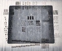
These three processes for creating step stencils result in different textures within the stepped area. The textures of the step stencils are shown below (Figure 4).
Figure 3: The micro-machining process to create a step stencil.
Experimental Methodology
A step stencil design was created with stepdown pockets of varying thicknesses. The base stencil thickness was 4.0 mils (101.6 microns) and the step-down pockets were 3.5 mils (88.9 microns), 3.0 mils (76.2 microns), 2.5 mils (63.5 microns), and 2.0 mils (50.8 microns) thick. Each step area was 1-inch square (25.4 mm) and the step design is shown below (Figure 5).
The thicknesses of each step pocket were measured using a FARO arm device. The measurements for each step technology were compared and contrasted.
An aperture pattern was created for the following components: 03015 metric, 01005, 0.3 mm BGA, 0.4 mm BGA, and 0.5 mm pitch QFNs. Apertures for each component were cut at varying distances from the step edges; 10, 20, 30, 40, and 50 mils. The intention was to determine how close solder paste could be printed to the step edge for each step stencil technology.
Figure 4: Textures of step areas for the three step technologies.
Figure 5: Step down pocket design.
Apertures were also cut into the center of each step area for comparison.
Each stencil was made with two sets of steps and apertures. One set of steps and apertures were coated with a fluoro-polymer nano (FPN) coating.
The effects of the FPN coating were compared to the uncoated part of the stencil on printing of solder paste. A 10-print study was run on each step stencil using a popular no clean, SAC305 Type 4 solder paste. The circuit boards used were bare copper clad material 0.062” (1.57 mm) thick. The printer used was a DEK Horizon 02i.
To read the full version of this article, which appeared in the December 2017 issue of SMT Magazine, click here.


