


 Elementary, Mr. Watson: The Design Matrix: Revealing the Hidden Truths of Reality
 Connect the Dots: Designing for the Future of Manufacturing Reality—Surface Finish
 The Pulse: Caught in the Crosshatch—A Cautionary Tale of Detective Work


Nano Dimension’s 3D Printing: Prototypes at the Push of a Button?
January 26, 2018 | Barry Matties, Publisher, I-Connect007Estimated reading time: 4 minutes
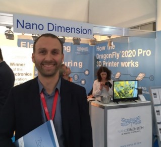
SICK AG is a global manufacturer of sensors and sensor solutions for industrial applications, with headquarters located in Waldkirch, Germany. After a demo of Nano Dimension’s new 3D printing machine at productronica, Barry Matties met with SICK’s Danny Wernet to discuss its pros and cons and get his overall impression of the technology. Are 3D prototypes really as simple as feeding in a Gerber file and pushing a button?
Barry Matties: Danny, can you share a little bit about your company and what you do?
Danny Wernet: We provide sensors and application solutions from factory automation to logistics automation and process automation, mainly for B2B. In this context we are one of the leading sensor manufacturers and a technology and market leader. Worldwide, we have about 8,000 employees, generating sales of about €1.4 billion.
Matties: What's your position?
Wernet: I am a business analyst in the electronics production in Waldkirch, which is in Southwest Germany.
Matties: We’re standing here looking at a Nano Dimension system for rapid prototypes. How does SICK take care of its customers’ prototype needs?
Wernet: We buy PCBs in the traditional way. If we need some PCBs for prototyping, we buy them in the market. SICK doesn’t produce PCBs.
Matties: For a few pieces, right? For three to five pieces.
Wernet: Yes, a few pieces. We produce relatively complex boards what results in a delivery time of between one and three weeks for these PCBs. This time is lost in order to reduce throughput time for assembly. Rapid prototyping of PCB could be a chance to offer R&D assemblies within a period of a few days. This might reduce time to market and provide competitive advantage. That's the issue to do it on our own.
Nano Dimension’s system is capable of printing one or two samples a day. It seems that batches with higher quantities cannot be produced economically yet.
Matties: So this is clearly just a single board.
Wernet: It is, obviously the system delivers samples in the short run which can be used to verify circuit design. To do the industrialization in production, we need some more…
Matties: Horsepower.
Wernet: Of course. In case R&D needs one or two prototypes to do some electrical measurement, it might be a solution. Coming to productronica, one of our goals was to get more information in order to speak internally about the next steps.
Matties: After the demonstration here, what's your impression? What did you walk away with?
Wernet: The technology is very interesting and will potentially cover a relevant part of the market share of PCB manufacturing in the future. As an internal electronics manufacturer for SICK’s PCBAs, we offer the complete value-added chain from accompanying the earliest steps of R&D to series production to our internal customers. Therefore, the rapid prototyping of PCBs offers us possibilities that we did not have in the past.
Matties: What were the drawbacks that you saw in the demonstration? Things that may concern you about this?
Wernet: The system is new in the market and there is little experience. Design rules have to be developed first, before the printed PCBs can be used as a sample with similar characteristics as later on in series production. There is always a risk being the first to use a new technology.
The system’s performance can be seen as a drawback, too. So, one board, depending on size and thickness, is printed up in approximately 5-15 hours; this needs to be reduced in the future.
Matties: What were the greatest benefits that you saw?
Wernet: As already mentioned, first of all, the reduction of procurement lead time for the PCB is the greatest benefit. From a production point of view, the technology itself is an advantage. I was wondering about how to do the programming, how to do the handling, the maintenance, and the service. As far as I can evaluate these issues, all of them seem to be manageable and are less extensive as I expected.
Matties: I agree, and I think the speed barrier is only a matter of time, right?
Wernet: Sure. The speed of the system and output will increase. Another issue to mention is the soldering temperature. The printed materials cannot withstand the soldering process with standard lead-free alloys with a melting point of about 220°. There are lead-free alternatives for low-temperature soldering, of course. However, it is recommended to solder these alloys using vapor phase technology which comes along with another investment and the need to increase production knowledge.
Matties: You'd have to change the process to make this work in your facility.
Wernet: At the moment, we do not have experience in vapor phase soldering. Investment in a laboratory vapor phase system is relatively low, but the process needs to be developed.
Matties: Now in terms that the way that the process works, it looks like you upload your Gerber, and you press a print button. And hours later, you have a completed prototype.
Wernet: That’s the ways Nano Dimension’s technicians presented the process. Everybody has Gerber; it's a kind of the industry standard. The operator has to define the thickness of each layer only. I do not think that it's an issue.
Matties: I know it's a process. The one good question you had during their presentation was the shelf life, or the life of the material, and it seems like the answer was a bit surprising to you.
Wernet: I'm not yet an expert in 3D printing, but we do a lot of dispensing, and there we are not familiar with a pot life of six months.
Matties: Right, you were expecting six hours.
Wernet: Or something like this. It's not an issue. We do dispensing, and there we have to do massive cleaning of the heads. As I said, I'm not an expert in inkjet and 3D, but I was positively surprised about the pot life and the two hours per week of maintenance. That was a really good issue that was not expected.
Matties: Is there anything that we haven't discussed that you would like to talk about?
Wernet: Of course, for curing, Nano Dimension uses infrared for one material and UV for the other. In order to increase process reliability, I would prefer one curing system. Another issue for me is that everything—process, machinery and auxiliary materials—is coming only from Nano Dimension; this might be a risk, and it has to be considered before the investment is made.
Matties: Nano Dimension mentioned the distributors, but it sounds like distributors are their market, right? It's all proprietary.
Wernet: Someone has to be first.
Matties: Well, congratulations on being here, and thank you for sharing your thoughts.
Wernet: Thank you.
Suggested Reading
Printing PCBs...In Your Office!
The days of producing a PCB prototype with a 3D printer may not be as distant as you think. Barry Matties spoke with Simon Fried of Nano Dimension about how 3D printing is becoming a reality, and how this disruptive technology will change the way designers produce rapid prototypes.
Share on:


Testimonial
"In a year when every marketing dollar mattered, I chose to keep I-Connect007 in our 2025 plan. Their commitment to high-quality, insightful content aligns with Koh Young’s values and helps readers navigate a changing industry. "
Brent Fischthal - Koh YoungSuggested Items
Indium Experts to Address Data Center Thermal Management and Sintering Standards at SMTA Conference
05/13/2026 | Indium CorporationAs a leading materials provider for the advanced electronic packaging market, Indium Corporation® experts will share their technical insight and knowledge on two critical industry topics—data center thermal management and sintering protocols—at the SMTA Electronics in Harsh Environments Conference, May 19-21, in Amsterdam, Netherlands.
KYZEN to Focus on Aqueous and Stencil Cleaning Solutions at SMTA Juarez Expo and Tech Forum
05/12/2026 | KYZENKYZEN, the global leader in innovative environmentally friendly cleaning chemistries, will exhibit at the SMTA Monterrey Expo & Tech Forum scheduled to take place on Thursday, May 21 at Injectronics Convention Center in Ciudad Juarez, Chihuahua.
Knocking Down the Bone Pile: Precision Milling of Underfilled Surface-mount Components
05/13/2026 | Nash Bell -- Column: Knocking Down the Bone PileUnderfill is a polymeric material used to fill the gap between a printed circuit board and the underside of surface-mount area-array packages such as BGA, QFP, and QFN devices, thereby surrounding and protecting the solder interconnections. This material increases the component's reliability when subjected to mechanical impacts and shocks by distributing forces.
BGA Technology Expands Inspection Capabilities with Creative Electron TruView X-ray System
05/08/2026 | BGA TechnologyBGA Technology, a leading provider of advanced electronics testing and inspection services, has enhanced its inspection capabilities with the addition of a Creative Electron TruView™ Simplex X-ray system at its Holbrook, New York facility.
AQUANOX A4727 and A4625 Lead KYZEN Offerings at SMTA Oregon Expo and Tech Forum
05/06/2026 | KYZENKYZEN, the global leader in innovative environmentally responsible cleaning chemistries, will exhibit at the SMTA Oregon Expo and Tech Forum scheduled to take place Thursday, May 19 at the Wingspan Event and Conference Center in Hillsboro, Oregon.