-
- News
- Books
Featured Books
- design007 Magazine
Latest Issues
Current IssueProper Floor Planning
Floor planning decisions can make or break performance, manufacturability, and timelines. This month’s contributors weigh in with their best practices for proper floor planning and specific strategies to get it right.
Showing Some Constraint
A strong design constraint strategy carefully balances a wide range of electrical and manufacturing trade-offs. This month, we explore the key requirements, common challenges, and best practices behind building an effective constraint strategy.
All About That Route
Most designers favor manual routing, but today's interactive autorouters may be changing designers' minds by allowing users more direct control. In this issue, our expert contributors discuss a variety of manual and autorouting strategies.
- Articles
- Columns
- Links
- Media kit
||| MENU - design007 Magazine
EMA Enhances OrCAD Capture Cloud with 14 Million-Part Ultra Librarian Database
January 30, 2018 | EMA Design AutomationEstimated reading time: 2 minutes
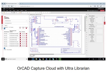
EMA Design Automation has integrated OrCAD Capture Cloud with Ultra Librarian, providing electronics engineers with a cloud-based design tool that is fully scalable to a professional, production-ready printed circuit board (PCB) design solution.
“Existing online design tools either lock users into a specific PCB manufacturer or don’t scale to a production-ready design process,” said Manny Marcano, president and CEO of EMA. “Integrating OrCAD Capture Cloud and Ultra Librarian provides designers with a cloud-based OrCAD Capture schematic entry tool and a comprehensive library of symbols, footprints, and 3D models that works with a proven PCB design suite for high-quality results.”
OrCAD Capture Cloud is a free, web-based subset of the OrCAD Capture schematic design tool from Cadence. The tool is accessed through a web browser and allows users to store their designs privately in the cloud. Users who already have the desktop version of OrCAD Capture will have both upload and download capabilities, giving them the ability to work in the cloud or on the desktop. “Designers aren’t always at their desk, so they may not have access to their work computer,” said Marcano. “With OrCAD Capture Cloud, designers can access their designs anywhere and on almost any computer, including Linux and Mac computers.”
Adding Ultra Librarian to OrCAD Capture Cloud solves the typical library problem by including direct access to the Ultra Librarian online library of over 14 million components. This gives designers drag-and-drop capabilities from the largest ECAD library in the industry. From within the OrCAD Capture Cloud environment, a user can search for parts, preview various results, and then place the schematic symbol directly onto a schematic page. The placed symbol’s properties include the appropriate footprint name, so that later work with OrCAD PCB Editor on the desktop has the correct information for placement and routing. This use of pre-built and validated library parts will both reduce errors and accelerate the design process.
“People using free tools typically have translation failures when the time comes to move to a professional level toolset,” added Marcano. “OrCAD Capture Cloud extends OrCAD’s desktop scalability to provide a seamless solution, eliminating this problem, while also adding more capabilities for professional level designers.”
About EMA Design Automation, Inc.
EMA Design Automation is a trailblazer in product development solutions offering a complete range of EDA tools, PLM integrations, services, training, and technical support. EMA is a Cadence Channel Partner serving all of North America. EMA develops Ultra Librarian, TimingDesigner, CircuitSpace, CIP, EDABuilder, and a host of custom solutions to enhance the OrCAD products, and all are distributed through a worldwide network of value added resellers. EMA is a privately held corporation headquartered in Rochester, New York. For more information, click here.
Testimonial
"Our marketing partnership with I-Connect007 is already delivering. Just a day after our press release went live, we received a direct inquiry about our updated products!"
Rachael Temple - AlltematedSuggested Items
Global PCB Connections: Understanding the General Fabrication Process—A Designer’s Hidden Advantage
08/14/2025 | Markus Voeltz -- Column: Global PCB ConnectionsDesigners don’t need to become fabricators, but understanding the basics of PCB fabrication can save you time, money, and frustration. The more you understand what’s happening on the shop floor, the better you’ll be able to prevent downstream issues. As you move into more advanced designs like HDI, flex circuits, stacked vias, and embedded components, this foundational knowledge becomes even more critical. Remember: the fabricator is your partner.
The Art and Science of PCB Floor Planning: A Comprehensive Guide
08/14/2025 | Cory Grunwald and Jeff Reinhold, Monsoon SolutionsPCB design is an intricate and crucial part of developing electronic products. One of the foundational stages of PCB design is floor planning, a phase where the placement of components and the flow of signals are meticulously mapped out. A good floor plan ensures that the PCB performs well, is easy to manufacture, and meets all mechanical and electrical requirements. We’ll explore the essential aspects of floor planning, from its objectives and process to the challenges that designers face.
EnSilica Establishes New EU Mixed-Signal Design Centre in Budapest, Hungary
08/12/2025 | EnSilicaThe facility strengthens EnSilica’s presence in the European Union and taps into Budapest’s deep technology ecosystem, which hosts numerous leading automotive and industrial multinationals. This expansion will increase the Group’s global headcount to around 210 employees.
Happy’s Tech Talk #41: Sustainability and Circularity for Electronics Manufacturing
08/13/2025 | Happy Holden -- Column: Happy’s Tech TalkI attended INEMI’s June 12 online seminar, “Sustainable Electronics Tech Topic Series: PCBs and Sustainability.” Dr. Maarten Cauwe of imec spoke on “Life Cycle Inventory (LCI) Models for Assessing and Improving the Environmental Impact of PCB Assemblies,” and Jack Herring of Jiva Materials Ltd. spoke on “Transforming Electronics with Recyclable PCB Technology.” This column will review information and provide analysis from both presentations.
Elementary, Mr. Watson: Why Your PCB Looks Like a Studio Apartment
08/13/2025 | John Watson -- Column: Elementary, Mr. WatsonIn November 2022, I wrote a column called "Is Your Bathroom in the Kitchen?" This piece related a bizarre real estate listing that emerged out of St. Louis that had architects scratching their heads and interior designers cringing. Nestled in the historic Central West End sat a 200-square-foot apartment that completely defied logic. It wasn't the size that raised eyebrows, it was the layout. Here's the kicker: While that's rare in real estate, it's shockingly common in PCB design.