-
- News
- Books
Featured Books
- design007 Magazine
Latest Issues
Current IssueMechatronics
Our expert contributors discuss the advent of mechatronics in PCB design, the challenges and opportunities this creates for circuit board designers, and the benefits—to the employee and the company—of becoming a mechatronics engineer.
Creating a Culture of Collaboration
PCB designers could learn quite a bit from NASA and the private companies that develop spacecraft: Every one of these vehicles is a testament to the value of collaboration among disparate stakeholders. Without a collaborative culture, the rocket might never get off the ground.
Breaking High-speed Material Constraints
Do you need specialty materials for your high-speed designs? Maybe not. Improvements in resins mean designers of high-speed boards can sometimes use traditional laminate systems. Learn more in this issue.
- Articles
- Columns
Search Console
- Links
- Events
||| MENU - design007 Magazine
iCD Introduces New Materials Planner Software
July 2, 2018 | ICDEstimated reading time: 1 minute
![](https://iconnect007.com/application/files/1416/3125/6722/iCD.jpg)
In-Circuit Design Pty Ltd (iCD), Australia, developer of the iCD Design Integrity software, has released the new iCD Materials Planner software to add to the Stackup Planner functionality. This will be rolled out to iCD support customers as an update to their current software.
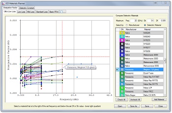
The Dielectric Materials Library, which complements the iCD Stackup Planner, has
- Over 33,000 rigid and flexible materials up to 100GHz
- Produced by over 60 different manufacturers
- Containing over 700 series of materials
So, it is often a daunting task to ascertain which is the best material for an application. The iCD Materials Planner allows you to compare dielectric materials based on manufacturer, fabricator, frequency, dissipation factor (loss) and dielectric constant. This enables the designer to make an informed decision on which material is best for his application.
Generally the selection metric, for dielectric materials, is the amount of loss that a transmission line can tolerate and this is proportional to the frequency and rise time of the signals. The iCD Materials Planner is subdivided into five default TABs which gives the novice high-speed PCB designer a heads-up as to what to select for his application.
- Ultra Low Loss (Df ≤ 0.005)
- Low Loss (0.005 < Df < 0.010)
- Mid Loss (0.010 < Df < 0.015)
- Standard Loss (0.015 < Df < 0.02)
- Basic FR-4 (Df ≥ 0.02)
This is similar to a typical competitive analysis that a material manufacturer may present for, say, Isola vs Ventec and Rogers, but it is far more comprehensive, with over 60 vendors and 700 series of materials to choose from. Alternatively, a profile for each PCB fabricator that you usually deal with can be set up. This will display the complete range of materials that each Fab shop stocks ranging from basic FR-4 to low loss materials. This also enables the comparison of competitive Fab shop capabilities.
Watch below for a quick demonstration video of the iCD Materials Planner:
About In-Circuit Design Pty Ltd
In-Circuit Design Pty Ltd, based in Australia, developer of the iCD Design Integrity software incorporating the iCD Stackup, PDN and CPW Planner software, is a PCB Design Service Bureau and specialist in board level simulation. For further information or to download a free evaluation of the software, please click here.
Suggested Items
Looking For That Perfect Job? Check Out jobCONNECT007
07/25/2024 | I-Connect007 Editorial TeamThere are a lot of open positions in this industry today. But where do you begin to look? We have the answer: jobCONNECT007, your guide to career opportunities in the electronic industry. In jobCONNECT007, you’ll find job openings that span the entire circuit board supply chain. Whether you’re involved in design, fabrication, assembly, test, or material development or distribution, this handy resource can help you get on your way to a new gig.
Strip Etch Strip: Episode 9 of On the Line With... Designing for Reality Podcast Now Available
07/25/2024 | I-Connect007Don't miss the latest episode of "On the Line With... Designing for Reality," where we walk through the PCB manufacturing process. At this stage, we have a panel made up of all the internal layers laminated together, through-holes drilled, and the outer layer copper features covered with a protective layer of tin.
Ventec Giga Solutions & Hi-Print Team up to Launch World's First 3-Color Inkjet Printing Solution
07/24/2024 | Ventec International GroupVentec Giga Solutions, Ventec’s value-added PCB equipment division, and leading inkjet printer manufacturer Hi-Print have teamed up to launch the industry’s most cutting-edge inkjet printer for solder mask technology.
Ian Walsh Appointed as Sondrel’s Regional VP for America
07/23/2024 | SondrellSondrel, a leading provider of ultra-complex, custom chips for leading global technology brands, has appointed Ian Walsh as its Regional VP for America, with the responsibility of growing Sondrel’s US semiconductor business from its new Silicon Valley offices in Santa Clara, CA.
LG Accelerates Smart Factory Solutions Business Integrating AI with 66-year Manufacturing Expertise
07/23/2024 | LGLG Electronics is advancing its smart factory solutions business by integrating artificial intelligence (AI) and digital transformation (DX) with its extensive 66-year history of manufacturing and production expertise.