


 Beyond Design: Skip-layer Routing—The Waveguide Structure That Makes 224G Possible
 Designers Notebook: Old vs. New School System-level Packaging—Flip-Chip to Chiplets
 Elementary, Mr. Watson: Builders of the Dream


WestDev Ltd. launches the next level of progression in its Pulsonix product with the release of version 10.0.
The latest release of Pulsonix expands its product portfolio with intelligent interactive editing within the 3D design environment. By enabling the co-design of the PCB within the 2D PCB and 3D environments, Pulsonix shortens the time to market with a more productive workflow and reduces costly errors.
The new interactive 3D design environment is complimented by new interactive functionality enabling dynamic Copper Pouring and shape healing. Automatic Pad Style Naming has also been introduced to ensure maximum efficiency for the user.
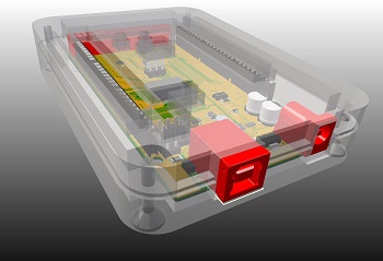
Interactive PCB and 3D Design Environment
Version 10 allows Mechanical enclosures to be integrated into the native Pulsonix 3D environment for modelling and critical clash detection. This tight integration alerts the engineer where items violate the rules defined. Once alerted, the offending item can then be moved directly from within the 3D Editor in Pulsonix and all changes automatically updated in the PCB design.
With both the detection of physical collisions between enclosures and components, and the subsequent resolution to a legal state, Pulsonix allows engineers to design more intelligently and efficiently, without needing to continually request updates on component positions from their mechanical CAD colleagues, thus saving valuable design time.
In today’s world of multi-disciplined facets and engineering demands, the new Pulsonix clash detection functionality significantly closes the gap between the electronics and the mechanical design environments.
New 3D Functionality Summary:
- Import Mechanical enclosures into the Pulsonix 3D environment
- Move components and enclosures in 3D Design
- Adhere to design rules for movement and placement of components
- Clash detection and resolution between Components and Enclosures
Dynamic Copper Pour
In addition to the 3D functionality, Pulsonix 10.0 also introduces the ability to dynamically repour copper areas during editing. This saves critical design time without the need to manually repour copper areas; instead, routing a track through the copper shape or moving a design item, such as a component or via, will automatically ‘heal’ the copper, all performed dynamically whilst obeying the design rules. With new zonal shape algorithms used in Pulsonix 10.0, only ‘damaged’ areas of copper are repaired making the healing much faster on large designs or designs with many complex poured areas.
Automatic Pad Naming Conventions
Style Naming Rules enable users in Pulsonix 10.0 to automatically comply to their company standards or with industry standard rules such as the IPC standard. A naming standard can be defined within a Technology file, this is then adhered to whenever a new style is created by the user. Although Style Naming rules can be applied to any item style, it is particularly useful for Pad Styles where the name requires a standard naming style applied to it, as would be the case for the IPC standard.
About Pulsonix Overview
Introduced in 2001, Pulsonix EDA software has made its mark to set the standard for high-performance Schematic design capture, Simulation, PCB layout and autorouting. Developed by a dedicated in-house team, each release demonstrates how the fast-growing Pulsonix product is introducing key features to win new business and offer users flexible and highly compatible software that meets the demands of PCB design today.


