


 Driving Innovation: Mechanical and Optical Processes During Rigid-flex Production
 It’s Only Common Sense: Your Biggest Competitor Is Complacency
 The Chemical Connection: Onshoring PCB Production—Daunting but Certainly Possible


Atoms Use Tunnels to Escape Graphene Cover
November 2, 2018 | Leiden UniversityEstimated reading time: 2 minutes
Graphene has held a great promise for applications since it was first isolated in 2004. But we still don’t use it in our large-scale technology, because we have no way of producing graphene on an industrial scale.
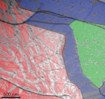
Image Caption: LEEM image of a graphene layer grown on a silicon carbide substrate. A red color indicates the presence of hydrogen atoms sandwiched between graphene and silicon carbide. The dark lines indicate strained regions in the graphene. The surrounding white areas show where the hydrogen atoms already left the interface. This shows that the lines act as tunnels where the hydrogen flows away faster.
Leiden physicists have now visualized for the first time how atoms behave in between graphene and a substrate. This insight could be instrumental for future implementations of industrial graphene production.
In 2004, scientists managed to isolate a single layer of carbon atoms from a block of graphite. Since then, this so-called graphene layer has been praised for its high potential for all sorts of promising applications. It would enable high-speed transistors, economic electrical cars and delicate sensors. So fast-forward to 2018, graphene is now the dominant building block of our computers, cars and gadgets, right? Wrong. There are still few large-scale graphene applications. The problem is that we haven’t figured out a way to produce graphene in high quality on the right substrate on an industrial scale.
Hydrogen Atoms
Though scientists do have an idea for large-scale production. If they heat silicon carbide to almost 2,000 °C, a graphene layer grows on its surface. However, they need to make sure that the desired properties of the graphene are not disturbed by the substrate. Inserting hydrogen atoms in between the graphene and silicon carbide isolates the graphene and leaves it intact as a single layer material. Leiden physicist Sense Jan van der Molen and his research group have now visualized for the first time how those atoms behave underneath the graphene.
Strained
The researchers, including postdoc Johannes Jobst and PhD candidate Tobias de Jong, used their low-energy electron microscope (LEEM) to study what happens to hydrogen atoms sandwiched between graphene and silicon carbide. They spotted lines where the graphene layer is strained. The hydrogen atoms use the lines as tunnels where they can escape more easily, whereas they stay put much longer under the graphene’s smooth regions between these lines. ‘The reversed process is widely used in research to decouple the graphene from the substrate,’ says Jobst. ‘But it was not clear how the hydrogen moves at the interface. We showed that hydrogen gas can be blown into those tunnels so that it will spread quickly underneath the graphene layer in the form of individual atoms.’
Share on:


Testimonial
"We’re proud to call I-Connect007 a trusted partner. Their innovative approach and industry insight made our podcast collaboration a success by connecting us with the right audience and delivering real results."
Julia McCaffrey - NCAB GroupSuggested Items
TRI to Unveil New High-Throughput AOI and AXI at productronica 2023
09/15/2023 | TRITest Research, Inc. (TRI), the leading test and inspection systems provider for the electronics manufacturing industry, will join productronica 2023, which will be held at Messe München Center from November 14 – 17, 2023.
UK Space Agency Launches Consultation on Variable Liability Limits for Orbital Operations
09/15/2023 | UK Space AgencyThe proposals from the UK Space Agency follow a review into the UK’s approach to setting the amount of an operator’s liability in licences for orbital operations, a key commitment of the government’s National Space Strategy.
MediaTek Successfully Develops First Chip Using TSMC's 3nm Process, Set for Volume Production in 2024
09/14/2023 | MediaTekMediaTek and TSMC announced that MediaTek has successfully developed its first chip using TSMC's leading-edge 3nm technology, taping out MediaTek’s flagship Dimensity system-on-chip (SoC) with volume production expected next year.
MKS’ Atotech to Participate in IPCA Expo 2023
09/14/2023 | MKS’ AtotechMKS’ Atotech, a leading surface finishing brand of MKS Instruments, will participate in the upcoming IPCA Expo at Bangalore International Exhibition Centre (BIEC) and showcase its latest PCB manufacturing solutions from September 13 – 15.
Comtech Unveils New BRIDGE Solutions to Increase Access to Global Hybrid Connectivity
09/12/2023 | Business WireComtech launched its new blended, resilient, integrated, digital, global, end-to-end (BRIDGE) connectivity solutions. Comtech’s BRIDGE solutions provide portable, adaptable, full-service communications networks that can be established in a matter of hours and help “bridge the gap” for traditional satellite and terrestrial infrastructures.