


 Elementary Mr. Watson: Running the Signal Gauntlet
 The Shaughnessy Report: Winning the Signal Integrity Battle
 Connect the Dots: How to Avoid Five Common Causes of Board Failure


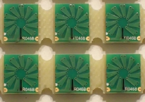
Embedded Inductors with Laser Machined Gap
December 17, 2018 | Jim Quilici, Radial ElectronicsEstimated reading time: 14 minutes
Energy efficiency is a major driver in the evolution of electronics and electronics packaging. To manage power consumption, portable appliances such as smartphones, tablets, e-readers, etc., often use multiple supply voltages and DC/DC converters. Most are based on switch mode power conversion (SMPC). In a power converter, inductors and transformers are used to temporarily store energy during switching cycles. They also have the function of filtering noise. The power magnetics are often the largest and most expensive devices in the circuit. Integrating the magnetics into either a power converter module or system board can significantly reduce size and cost of the power converter function.
Embedded magnetics offer a means for integrating the magnetic functions into a PCB substrate. Ferromagnetic cores are embedded into a PCB substrate, and the inductive windings are implemented using photolithography and standard PCB processes. Rather than building one-at-a-time, devices are arrayed on a PCB panel and fabricated using automated and batch process. In most instances, the embedded core will be a ring shaped (toroid), since this is the most efficient shape in terms of delivering high inductance per turn and containing the induced magnetic flux. Additionally, toroids are a relatively easy shape to manufacture and generally inexpensive compared to other core shapes. Common materials are pressed ceramic ferrites and tape-wound amorphous metals.
Figure 1: Embedded magnetic construction.
As indicated above, inductors and transformers are used in power converters to temporarily store energy during a switching event. A key metric of magnetic materials is their ability to store magnetic flux energy. When current is driven through a conductor wound around a magnetic core material, it produces a magnetic field (H) which induces a magnetic flux (B) in the underlying core material. The current energy is temporarily converted to magnetic flux and stored within the magnetic core. The flux, B, is essentially the field density within the core. B has units of Tesla (T) (or Gauss, G; 10,000 G = 1 T) and H is the measure of magnetizing field strength and has the units of Oersteds (Oe; 1 A/m = 4 x 10⁻³ Oe). B and H are closely related to voltage and current, where the flux density is proportional to the applied voltage and the magnetizing force, H, is proportional to current. The relationship between the field and flux is tied by the materials permeability, μ.
(1) B = μ H
Flux density may also be expressed in terms of inductance and drive current, as characterized through the relationship:
(2) B = LI/NAc
where L is the inductance, I is the drive current, N is the number of windings and Ac is the cross section area of the core.
Designers often use the B-H curve to analyze the relationship between the drive voltage and drive current. Figure 2 identifies that magnetic materials have a flux saturation level, BSAT, which is the state where the magnetic core has reached peak flux density. At that point, the core cannot store more energy, regardless of the amplitude of drive voltage. For ferrite materials, saturation occurs in the range of 0.350 to 0.550 T (Tesla is a unit of magnetic flux density.), depending on the composition. Cores with high permeability will saturate with modest currents. To allow higher drive currents, a gap is often introduced into the magnetic flux path. This effectively reduces the permeability of the core material and results in a reduction of the inductance of the windings. As depicted in Figure 2, gapping the core flattens out the B-H curve. Reducing the inductance allows the core to store energy from higher drive currents.
Figure 2: Typical B-H graph for an ungapped and gapped ferrite core.
A gap is produced by placing a small cut through the core. Gapping is a common method for reducing the inductance and enabling the core to be driven at higher currents before reaching saturation. It also serves to stabilize the performance of a core over different operating temperatures and drive currents. Basically, gapping the core reduces the effective permeability. The relative permeability for a gapped core can be calculated by the equation:
(3) μr' = μr / (1 +( g x μr /le)
where g is the gap distance and le is the path length of the flux around the circumference of the core. In many instances, the reduction in permeability by gapping will exceed 10x. It may seem counterproductive to create materials and core structures with high permeability and then diminish them with a gap. However, this is necessary to add stability and allow higher drive currents. There is always the option of using powdered iron core materials, which are often described as having a distributed gap. These materials generally have permeability’s less than 100 and are generally more expensive due to the precious metals used in their construction and limited number of suppliers. With conventional ferrites, we can apply a gap to achieve permeability values between 100 and 1000, which reduces the number of windings required to achieve a specific inductance. Reducing the number of windings is beneficial in reducing resistance loss in the windings. Also powdered iron materials generally exhibit higher core loss which can also impact the power converters efficiency. Core losses are a result of an alternating magnetic field in a core material. The core losses are due to hysteresis, eddy current and residual losses in the core material and is dissipated as heat.
Figure 3: Example of a gapped toroid.
Figure 4 shows a typical graph of permeability vs. temperature for a 2000 permeability manganese zinc (MnZn) material, which is typically used for power applications. Here, we see wide variations over temperature. Gapping the core reduces the permeability to about 350 and flattens out the characteristics over the full temperature range. This is important for applications that need to perform to at temperatures below 0°C.
This brings us to a design methodology. Once the designer determines the inductance required for an application, it is then a matter of over designing for much higher inductance, in anticipation that the inductance will be diminished after the core has been gapped.
Figure 4: Ferrite permeability vs. temperature (1500 permeability @ 25°C).
For power converters, embedded magnetics are useful in applications ranging up to 60 W. The power capability is primarily dictated by core sizes that are suitable for embedding into a PCB substrate. The PCB construction is limited by the PCB thickness and height (thickness) of the core. Practical applications include power to a microprocessor, battery chargers and LED lighting. There are many semiconductor SMPC controllers on the market tailored specifically for these applications. Most of these devices operate with switching speeds ranging from 500 kHz to 2 MHz. At these switching speeds, inductors in the range of 1 µH to 10 µH are commonly used. For this investigation, a test coupon was designed with indictors ranging from 2.2 µH to 10 µH. The 10 µH configuration is the focus of this paper. Generally, for power applications, it is best to select MnZn ferrite materials with permeability in the range of 2K to 3K, due to their core loss properties. In this gapping experiment, however, cores with 5K permeability were selected simply because this value was available in the author’s inventory. This difference in permeability is not significant in this particular experiment. Once the gap is applied, the core’s inductance per turn is dominated by the gap with. The differences in the initial permeability only accounts for minor difference in the final inductance.
Page 1 of 3
Share on:


Testimonial
"Advertising in PCB007 Magazine has been a great way to showcase our bare board testers to the right audience. The I-Connect007 team makes the process smooth and professional. We’re proud to be featured in such a trusted publication."
Klaus Koziol - atgSuggested Items
Trouble in Your Tank: Implementing Direct Metallization in Advanced Substrate Packaging
09/15/2025 | Michael Carano -- Column: Trouble in Your TankDirect metallization systems based on conductive graphite are gaining popularity throughout the world. The environmental and productivity gains achievable with this process are outstanding. Direct metallization reduces the costs of compliance, waste treatment, and legal issues related to chemical exposure. A graphite-based direct plate system has been devised to address these needs.
Closing the Loop on PCB Etching Waste
09/09/2025 | Shawn Stone, IECAs the PCB industry continues its push toward greener, more cost-efficient operations, Sigma Engineering’s Mecer System offers a comprehensive solution to two of the industry’s most persistent pain points: etchant consumption and rinse water waste. Designed as a modular, fully automated platform, the Mecer System regenerates spent copper etchants—both alkaline and acidic—and simultaneously recycles rinse water, transforming a traditionally linear chemical process into a closed-loop system.
Driving Innovation: Depth Routing Processes—Achieving Unparalleled Precision in Complex PCBs
09/08/2025 | Kurt Palmer -- Column: Driving InnovationIn PCB manufacturing, the demand for increasingly complex and miniaturized designs continually pushes the boundaries of traditional fabrication methods, including depth routing. Success in these applications demands not only on robust machinery but also sophisticated control functions. PCB manufacturers rely on advanced machine features and process methodologies to meet their precise depth routing goals. Here, I’ll explore some crucial functions that empower manufacturers to master complex depth routing challenges.
Trouble in Your Tank: Minimizing Small-via Defects for High-reliability PCBs
08/27/2025 | Michael Carano -- Column: Trouble in Your TankTo quote the comedian Stephen Wright, “If at first you don’t succeed, then skydiving is not for you.” That can be the battle cry when you find that only small-diameter vias are exhibiting voids. Why are small holes more prone to voids than larger vias when processed through electroless copper? There are several reasons.
The Government Circuit: Navigating New Trade Headwinds and New Partnerships
08/25/2025 | Chris Mitchell -- Column: The Government CircuitAs global trade winds continue to howl, the electronics manufacturing industry finds itself at a critical juncture. After months of warnings, the U.S. Government has implemented a broad array of tariff increases, with fresh duties hitting copper-based products, semiconductors, and imports from many nations. On the positive side, tentative trade agreements with Europe, China, Japan, and other nations are providing at least some clarity and counterbalance.