


 Global Sourcing Spotlight: Making Global Sourcing Simple Again
 The Government Circuit: New Council Now Helps Shape Policy Decisions in the Electronics Supply Chain
 Learning With Leo: Soldering—The Interpretation Problem


An HZB team has fabricated and characterized a thin-film tandem solar cell made of perovskite and CIGSe. They relied on a simple, robust fabrication process that is also suitable for scaling up to large surface areas. The tandem solar cell is a fully thin film device with an impressive efficiency of 21.6%. With further improvements it might reach efficiencies above 30%.
Tandem solar cells consist of two semiconductors with different band gaps, enabling them to use a larger fraction of the solar spectrum for generating electricity. This concept is particularly successful when conventional absorber layers such as silicon or copper indium gallium selenide (CIGSe) are combined with the new metal-halide semiconductor perovskite. This is because perovskites convert the blue, high-energy portions of sunlight into electrical energy very efficiently, while silicon or CIGSe convert the red and near-infrared portions effectively.
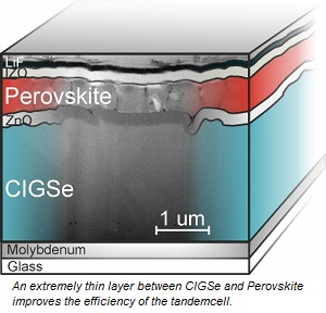
CIGSe and Perovskite Thin Films Combined
HZB researchers have now combined a thin-film solar cell made of CIGSe with a thin layer of perovskite. The CIGSe thin film was grown on a substrate, resulting in a CIGSe surface that is typically rough and irregular. This has made the application of the perovskite top cell using wet-chemical methods more difficult thus far.
Ultrathin Layer Improves Cell Efficiency
The HZB team in cooperation with Eindhoven University of Technology has now for the first time improved the properties of the tandem solar cell by applying an ultra-thin yet conformal intermediate layer to the CIGSe layer, then spin-coating the perovskite layer onto it at the HySPRINT lab of HZB. The tandem solar cell produced in this way converts 21.6% of the solar spectrum into electrical energy. This power conversion efficiency remains stable.
Manufacture Requires Minimal Energy
Although tandem cells made of silicon and perovskite achieve even higher efficiencies so far, theoretically, CIGSe perovskite tandem cells could also achieve these efficiencies. In addition, the new CIGSe perovskite tandem cell is a fully thin film device. This means that the new tandem cell is made from thin layers of CIGSe and perovskite so that the material and energy consumed during its manufacture are extremely low.
Mass Production Feasible
“This tandem cell was fabricated on a rough, untreated CIGS bottom cell, which simplifies manufacture and represents an enormous advantage in terms of mass production“, Prof. Dr. Rutger Schlatmann, Director of the HZB Institute PVcomB, points out.
The tandem solar cell was realised on an area of 0.8 square centimetres, which is considerably larger than the square-millimetre areas commonly used in laboratory research.
“Record values are only recognised for areas of one square centimetre or more, yet our cell area is just slightly below this threshold. Therefore, we now focus to certify this tandem solar cell efficiency and its enormous performance by an independent institution“, says Prof. Dr. Steve Albrecht, head of a Young Investigator Group at HZB, funded by the Federal Ministry for Education and Research (BMBF).
Outlook: Possible Efficiencies of Over 30%
Using electron microscopy and other measurements, first author Dr. Marko Jost, a postdoc in Steve Albrecht's team, and his colleagues analysed the conformal layer structure of the tandem cell and were also able to determine the contributions of the individual sub-cells to the performance of the tandem cell. Their study points out ways to further improve monolithic perovskite/CIGSe tandem cells and achieve efficiencies of over 30%.


