-

- News
- Books
Featured Books
- pcb007 Magazine
Latest Issues
Current Issue
The Hole Truth: Via Integrity in an HDI World
From the drilled hole to registration across multiple sequential lamination cycles, to the quality of your copper plating, via reliability in an HDI world is becoming an ever-greater challenge. This month we look at “The Hole Truth,” from creating the “perfect” via to how you can assure via quality and reliability, the first time, every time.

In Pursuit of Perfection: Defect Reduction
For bare PCB board fabrication, defect reduction is a critical aspect of a company's bottom line profitability. In this issue, we examine how imaging, etching, and plating processes can provide information and insight into reducing defects and increasing yields.

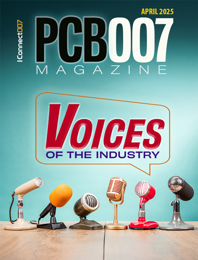
Voices of the Industry
We take the pulse of the PCB industry by sharing insights from leading fabricators and suppliers in this month's issue. We've gathered their thoughts on the new U.S. administration, spending, the war in Ukraine, and their most pressing needs. It’s an eye-opening and enlightening look behind the curtain.
- Articles
- Columns
- Links
- Media kit
||| MENU - pcb007 Magazine
Chemical Recycling as Part of a Zero-effluent Strategy
March 6, 2019 | Happy Holden, I-Connect007Estimated reading time: 1 minute
Green manufacturing methodologies for PCBs are becoming a global shift. Green efforts have been underway in the European Union for quite some time. Likewise, in the United States, new PCB manufacturers are building zero-waste, zero-effluent facilities and gaining certification as such. Furthermore, in China, government mandates are transforming the amount of pollutants tolerated from PCB manufacturing down to nearly zero or face forced relocation from populated areas.
In this article, I will examine some of the key areas of improvement in chemical recycling that you should consider as you move your fabrication facility toward green and zero effluent manufacturing. For the scope of this article, I will use GreenSource Fabrication’s New Hampshire facility as our primary example.
New Example of Green for Printed Circuit Fabrication
To build a new PCB manufacturing facility in New Hampshire, GreenSource had to guarantee the government that they would be zero-effluent. While engineering the concepts of no effluents and being mindful of Six Sigma and Lean principles, the process is fully automated with minimal process delays and no handling by employees, thus being an excellent example of Lean plus green! The two go hand-in-hand.
The new facility does not require waste permits because there were no water emissions. Water is recycled, as are many of the chemicals, reducing costs. The totally automated process requires only seven technicians to monitor the machinery and a total of 17 staff people for the entire multilayer facility. As seen in Figure 1, the bulk of the PCB processing is conducted in numerous automated machines connected by conveyors or AGVs.
Figure 1: The main high-volume PCB processes are automated on several conveyorized systems from the materials warehouse (an automated storage and retrieval system, or AS/RS) through final solder mask and fabrication.
This article originally appeared in the January 2019 issue of PCB007 Magazine, click here.
Suggested Items
SHENMAO Strengthens Semiconductor Capabilities with Acquisition of PMTC
07/10/2025 | SHENMAOSHENMAO America, Inc. has announced the acquisition of Profound Material Technology Co., Ltd. (PMTC), a premier Taiwan-based manufacturer of high-performance solder balls for semiconductor packaging.
KYZEN to Highlight Understencil and PCB Cleaners at SMTA Querétaro Expo and Tech Forum
07/09/2025 | KYZEN'KYZEN, the global leader in innovative environmentally responsible cleaning chemistries, will exhibit at the SMTA Querétaro Expo & Tech Forum, scheduled to take place Thursday, July 24, at Centro de Congresos y Teatro Metropolitano de Querétaro.
Driving Innovation: Direct Imaging vs. Conventional Exposure
07/01/2025 | Simon Khesin -- Column: Driving InnovationMy first camera used Kodak film. I even experimented with developing photos in the bathroom, though I usually dropped the film off at a Kodak center and received the prints two weeks later, only to discover that some images were out of focus or poorly framed. Today, every smartphone contains a high-quality camera capable of producing stunning images instantly.
Hands-On Demos Now Available for Apollo Seiko’s EF and AF Selective Soldering Lines
06/30/2025 | Apollo SeikoApollo Seiko, a leading innovator in soldering technology, is excited to spotlight its expanded lineup of EF and AF Series Selective Soldering Systems, now available for live demonstrations in its newly dedicated demo room.
Indium Corporation Expert to Present on Automotive and Industrial Solder Bonding Solutions at Global Electronics Association Workshop
06/26/2025 | IndiumIndium Corporation Principal Engineer, Advanced Materials, Andy Mackie, Ph.D., MSc, will deliver a technical presentation on innovative solder bonding solutions for automotive and industrial applications at the Global Electronics A


