


 Punching Out: How to Stay Focused in Business and M&A
 It’s Only Common Sense: Just Imagine…


In any conventional silicon-based solar cell, there is an absolute limit on overall efficiency, based partly on the fact that each photon of light can only knock loose a single electron, even if that photon carried twice the energy needed to do so.
Image Caption: Diagram depicts the process of “singlet fission,” which is the first step toward producing two electrons from a single incoming photon of light.
But now, researchers have demonstrated a method for getting high-energy photons striking silicon to kick out two electrons instead of one, opening the door for a new kind of solar cell with greater efficiency than was thought possible.
While conventional silicon cells have an absolute theoretical maximum efficiency of about 29.1 percent conversion of solar energy, the new approach, developed over the last several years by researchers at MIT and elsewhere, could bust through that limit, potentially adding several percentage points to that maximum output. The results are described today in the journal Nature, in a paper by graduate student Markus Einzinger, professor of chemistry Moungi Bawendi, professor of electrical engineering and computer science Marc Baldo, and eight others at MIT and at Princeton University.
The basic concept behind this new technology has been known for decades, and the first demonstration that the principle could work was carried out by some members of this team six years ago. But actually translating the method into a full, operational silicon solar cell took years of hard work, Baldo says.
That initial demonstration “was a good test platform” to show that the idea could work, explains Daniel Congreve PhD ’15, an alumnus now at the Rowland Institute at Harvard, who was the lead author in that prior report and is a co-author of the new paper. Now, with the new results, “we’ve done what we set out to do” in that project, he says.
The original study demonstrated the production of two electrons from one photon, but it did so in an organic photovoltaic cell, which is less efficient than a silicon solar cell. It turned out that transferring the two electrons from a top collecting layer made of tetracene into the silicon cell “was not straightforward,” Baldo says. Troy Van Voorhis, a professor of chemistry at MIT who was part of that original team, points out that the concept was first proposed back in the 1970s, and says wryly that turning that idea into a practical device “only took 40 years.”
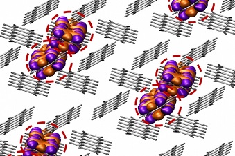
The key to splitting the energy of one photon into two electrons lies in a class of materials that possess “excited states” called excitons, Baldo says: In these excitonic materials, “these packets of energy propagate around like the electrons in a circuit,” but with quite different properties than electrons. “You can use them to change energy — you can cut them in half, you can combine them.” In this case, they were going through a process called singlet exciton fission, which is how the light’s energy gets split into two separate, independently moving packets of energy. The material first absorbs a photon, forming an exciton that rapidly undergoes fission into two excited states, each with half the energy of the original state.
But the tricky part was then coupling that energy over into the silicon, a material that is not excitonic. This coupling had never been accomplished before.
As an intermediate step, the team tried coupling the energy from the excitonic layer into a material called quantum dots. “They’re still excitonic, but they’re inorganic,” Baldo says. “That worked; it worked like a charm,” he says. By understanding the mechanism taking place in that material, he says, “we had no reason to think that silicon wouldn’t work.”
What that work showed, Van Voorhis says, is that the key to these energy transfers lies in the very surface of the material, not in its bulk. “So it was clear that the surface chemistry on silicon was going to be important. That was what was going to determine what kinds of surface states there were.” That focus on the surface chemistry may have been what allowed this team to succeed where others had not, he suggests.
The key was in a thin intermediate layer. “It turns out this tiny, tiny strip of material at the interface between these two systems [the silicon solar cell and the tetracene layer with its excitonic properties] ended up defining everything. It’s why other researchers couldn’t get this process to work, and why we finally did.” It was Einzinger “who finally cracked that nut,” he says, by using a layer of a material called hafnium oxynitride.
The layer is only a few atoms thick, or just 8 angstroms (ten-billionths of a meter), but it acted as a “nice bridge” for the excited states, Baldo says. That finally made it possible for the single high-energy photons to trigger the release of two electrons inside the silicon cell. That produces a doubling of the amount of energy produced by a given amount of sunlight in the blue and green part of the spectrum. Overall, that could produce an increase in the power produced by the solar cell — from a theoretical maximum of 29.1 percent, up to a maximum of about 35 percent.
Actual silicon cells are not yet at their maximum, and neither is the new material, so more development needs to be done, but the crucial step of coupling the two materials efficiently has now been proven. “We still need to optimize the silicon cells for this process,” Baldo says. For one thing, with the new system those cells can be thinner than current versions. Work also needs to be done on stabilizing the materials for durability. Overall, commercial applications are probably still a few years off, the team says.
Other approaches to improving the efficiency of solar cells tend to involve adding another kind of cell, such as a perovskite layer, over the silicon. Baldo says “they’re building one cell on top of another. Fundamentally, we’re making one cell — we’re kind of turbocharging the silicon cell. We’re adding more current into the silicon, as opposed to making two cells.”
The researchers have measured one special property of hafnium oxynitride that helps it transfer the excitonic energy. “We know that hafnium oxynitride generates additional charge at the interface, which reduces losses by a process called electric field passivation. If we can establish better control over this phenomenon, efficiencies may climb even higher.” Einzinger says. So far, no other material they’ve tested can match its properties.
The research was supported as part of the MIT Center for Excitonics, funded by the U.S. Department of Energy.


