


 The Marketing Minute: If Your Marketing Budget Gets Cut in Half, Then What?
 Punching Out: How Are the Big Boys in Electronics Doing?
 It’s Only Common Sense: Complexity Is the Enemy of Profit


First EIE Direct Imager at Electronic Interconnect: One Year Production Update
August 16, 2019 | First EIE SAEstimated reading time: 2 minutes
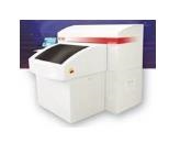
For more than a year, Electronic Interconnect Ltd. has been using the First EIE Direct Imager—EDI500 HV—in production at its Elk Grove Village, Illinois, location. The First EIE Direct Imager is fully manufactured in Switzerland, including the broad wavelength optical engine, which provides an operator-friendly user interface on a highly reliable platform while addressing advanced production needs.
Based on DMD technology, First EIE’s Direct Imager features a high-powered ultraviolet light source, which provides a full spectral range from 365 nm to 450 nm, allowing full compatibility with most resists and solder masks. The feature-rich software includes advanced local scaling or simple panel scaling; a high-resolution, fully automated target finder; exposable features down to 1-mil L/S; and real-time Z-axis auto-focus. The EDI500 addresses panel sizes up to 24″ x 27″ with a compact footprint, standard utility connections, and maintenance-friendly design.
Sanjay Shah, Electronic Interconnect COO, said, “I am very happy with this equipment. Now, I am sure that the light engine with the broad wavelength spectrum has many benefits for my exposure process with dry films, in particular with solder mask. I have seen a significant difference in the quality and finish of direct imaging as well as conventional mask exposed with the First EIE Direct Imager due to the broad UV spectrum. The exposing time with the direct imaging mask is quite impressive.”
About Electronic Interconnect
U.S. printed circuit board manufacturer Electronic Interconnect serves design engineers, OEMs, and contract manufacturers throughout the country. With over 30 years of experience, their customers have benefitted from unique technical advancements in areas such as thermal management, metal cladding, heavy copper, and solderability.
About First EIE
First EIE SA, Switzerland, provides outstanding equipment for leading markets seeking high-end imaging technologies. With its 512-beam optical engine, the latest generation of RP photoplotters achieves features down to 5 microns at 50000 dpi. The EDI Series for Direct Imaging enables the possibility to expose the all UV Photo sensitive substrates from Dry Film to Solder Mask including Legend.
Headquartered in southern California, all4-PCB is First EIE’s representative in North America.
Share on:


Testimonial
"The I-Connect007 team is outstanding—kind, responsive, and a true marketing partner. Their design team created fresh, eye-catching ads, and their editorial support polished our content to let our brand shine. Thank you all! "
Sweeney Ng - CEE PCBSuggested Items
Indium Experts to Address Data Center Thermal Management and Sintering Standards at SMTA Conference
05/13/2026 | Indium CorporationAs a leading materials provider for the advanced electronic packaging market, Indium Corporation® experts will share their technical insight and knowledge on two critical industry topics—data center thermal management and sintering protocols—at the SMTA Electronics in Harsh Environments Conference, May 19-21, in Amsterdam, Netherlands.
KYZEN to Focus on Aqueous and Stencil Cleaning Solutions at SMTA Juarez Expo and Tech Forum
05/12/2026 | KYZENKYZEN, the global leader in innovative environmentally friendly cleaning chemistries, will exhibit at the SMTA Monterrey Expo & Tech Forum scheduled to take place on Thursday, May 21 at Injectronics Convention Center in Ciudad Juarez, Chihuahua.
Knocking Down the Bone Pile: Precision Milling of Underfilled SMT Components
05/13/2026 | Nash Bell -- Column: Knocking Down the Bone PileUnderfill is a polymeric material used to fill the gap between a printed circuit board and the underside of surface-mount area-array packages such as BGA, QFP, and QFN devices, thereby surrounding and protecting the solder interconnections. This material increases the component's reliability when subjected to mechanical impacts and shocks by distributing forces.
BGA Technology Expands Inspection Capabilities with Creative Electron TruView X-ray System
05/08/2026 | BGA TechnologyBGA Technology, a leading provider of advanced electronics testing and inspection services, has enhanced its inspection capabilities with the addition of a Creative Electron TruView™ Simplex X-ray system at its Holbrook, New York facility.
AQUANOX A4727 and A4625 Lead KYZEN Offerings at SMTA Oregon Expo and Tech Forum
05/06/2026 | KYZENKYZEN, the global leader in innovative environmentally responsible cleaning chemistries, will exhibit at the SMTA Oregon Expo and Tech Forum scheduled to take place Thursday, May 19 at the Wingspan Event and Conference Center in Hillsboro, Oregon.