


 Fresh PCB Concepts: Engineering Copper Coin and Copper Pedestal Technology With IPC Design Interpretation
 Target Condition: Signal Integrity Without Borders
 Elementary, Mr. Watson: PCB Education in the Midst of the Storms


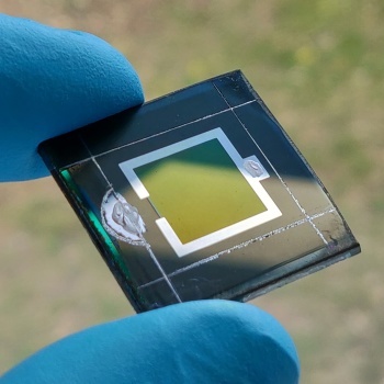
A team headed by Prof. Steve Albrecht from the HZB will present a new world-record tandem solar cell at EU PVSEC, the world's largest international photovoltaic and solar energy conference and exhibition, in Marseille, France on September 11, 2019. This tandem solar cell combines the semiconducting materials perovskite and CIGS and achieves a certified efficiency of 23.26%. One reason for this success lies in the cell’s intermediate layer of organic molecules: they self-organise to cover even rough semiconductor surfaces. Two patents have been filed for these layers.
Perovskite-based solar cells have experienced an incredibly rapid increase in efficiency over the last ten years. The combination of perovskites with classical semiconductor materials such as silicon and copper-indium-gallium-selenide (CIGS) compounds in tandem solar cells promises low-cost, high-performance solar modules for the future. However, losses at the electrodes between the two semiconductors considerably reduce the efficiency.
Record Efficiency: 23.26%
HZB physicist Prof. Steve Albrecht and his team now successfully established novel electrode coatings that greatly reduce these losses. They could produce a monolithic tandem solar cell from perovskite and CIGS that achieved an officially certified efficiency of 23.26%, which currently is a world record value. The tandem cell has an active area of one square centimetre and thus reaches another milestone, as perovskite CIGS tandem cells have so far been significantly smaller.
Self Assembled Monolayer
The contact layers consist of carbazole-based organic molecules coupled to phosphonic acid groups. These molecules arrange themselves into what are known as self-assembled monolayers (SAMs). These SAMs have highly favourable electro-optical properties and the self-assembly even leads to complete coverage of rough semiconductor surfaces.
Two Patents Filed
“The SAMs are strikingly simple and robust. This also allows them to be scaled up to industrial levels. In addition, they are compatible to a wide variety of substrates and their material consumption is extremely low”, explains Amran Al-Ashouri, PhD student in the Albrecht group and first author of the study. This work might further accelerate progress towards extremely inexpensive perovskite-based PV technologies. The group has now filed two patents and is currently in licensing negotiations.
Prof. Steve Albrecht heads the Perovskite Tandem Solar Cells Junior Research Group funded by the German Federal Ministry of Education and Research (BMBF). Work on the perovskite solar cells took place primarily in the Helmholtz HySPRINT Innovation Lab, while the SAMs were developed in close collaboration with Kaunas University of Technology (Lithuania), where the group of Prof. Vytautas Getautis synthesized the molecules. The CIGS layers are provided by the group of Dr. Christian Kaufmann, who heads the high efficiency CIGS activities at HZB and is supported by the SpeedCIGS project funded by the German Federal Ministry for Economic Affairs and Energy (BMWi).


