


 Beyond Design: Skip-layer Routing—The Waveguide Structure That Makes 224G Possible
 Designers Notebook: Old vs. New School System-level Packaging—Flip-Chip to Chiplets
 Elementary, Mr. Watson: Builders of the Dream


Zuken unveils advanced high-speed design features for its recently launched eCADSTAR connected PCB design platform. eCADSTAR Advanced HS extends eCADSTAR’s connected 3D PCB design capabilities with powerful high-speed routing tools, such as length and delay-based impedance and skew control and comprehensive constraint management capabilities. With the release of eCADSTAR Advanced HS, eCADSTAR is now available in four complementary bundles that can be easily combined to meet individual profiles.
“As products become more complex and connected, high-speed design is a key part of the design and manufacturability of printed circuit boards (PCBs). High-speed components and interfaces are at the heart of today’s smart and internet-connected products, and they demand advanced requirements for layout and routing,” says John Berrie, Signal Integrity Expert, Zuken Tech Center, Bristol. “eCADSTAR Advanced HS delivers those capabilities in an easy to use environment so that PCB designers can deliver exceptional high-speed design quality.”
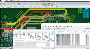
High-speed PCB design
The need to utilize high-speed design principles is becoming the norm rather than the exception—even if the clock-rates are not in the gigahertz range. Many of today’s common components like DDR3, DDR4 or DDR5 SDRAMs require high-speed PCB design practices to produce high-signal quality. As product performance increases and the need for device connectivity is pervasive, so is the need for high-speed constraint-driven PCB layout techniques.
eCADSTAR Advanced HS
With a consistent user interface from design entry through physical layout and a central constraint browser, eCADSTAR Advanced HS provides powerful built-in capabilities to address the complex details of critical high-speed layout and routing. Constraints can be specified both in the schematic, and the physical design tools, or as design rules stacks eCADSTAR’s built-in constraint browser. eCADSTAR’s high-speed capabilities include:
- Impedance controlled routing: In eCADSTAR, hardware engineers can constrain both single-ended and differential impedance to meet constraints on each board layer.
- Length, delay, and skew based routing: eCADSTAR works with both, length and delay constraints, including built-in simulation for detailed investigation of effects such as signal-to-signal coupling.
- Topology control: High-speed signals need a routing topology that adheres to specified constraints. eCADSTAR enables topology control with a wide selection of templates and instant visualization to make control as fast and reliable as possible.
- Handling of differential signals: In eCADSTAR differential signals can be routed with the assistance of automatic, clean end routing, specific design rules, and constraints.
Configurations and pricing
With modular bundles, eCADSTAR Base, Advanced 3D, Advanced HS, and Ultimate eCADSTAR can be configured in a wide variety of options to fit individual needs. eCADSTAR promotional pricing starts at under £2000 / €2200 EUR / $US2500.


