


 Fresh PCB Concepts: IPC-6012 Class 3 and High-reliability PCB Manufacturing
 Elementary, Mr. Watson: The Display Revolution, Now With Fewer Tiny Keys
 Beyond Design: Skip-layer Routing—The Waveguide Structure That Makes 224G Possible


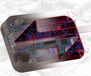
EMA Design Automation, a full-service provider and innovator of Electronic Design Automation (EDA) solutions, today announced CADSync™, providing a streamlined way to accurately pass high-fidelity design data and changes between Cadence PCB and SOLIDWORKS. “ This patent pending technology provides native bidirectional collaboration and traceability,” said Manny Marcano, president and CEO of EMA. “ Design teams can now work in concert for early communication and data sharing, enabling them to successfully launch mechatronic products on time and on budget.”
The current state of ECAD/MCAD 'collaboration' typically involves throwing large STEP files over the wall hoping each team can derive the data they need. This results in inaccuracy, miscommunication, delays, and even design re-spins. CADSync is the first and only native, bi-directional conduit between SOLIDWORKS and OrCAD®/Allegro® PCB Editor, providing a connection between ECAD and MCAD domains and eliminating the need for any middleware. PCB designers now have in-tool access to leverage native CAD data structures for maximum performance, efficiency, and accuracy, versus other solutions using common interchange formats.
CADSync includes a unique PCB toolkit for SOLIDWORKS which enables SOLIDWORKS teams to work on PCB features in their native design environment, while automatically capturing the data needed to properly specify changes and requirements in Cadence PCB. Since ECAD data is communicated to SOLIDWORKS using native solid parts, features, and assemblies, MCAD designers can also easily simulate and manipulate PCB elements in context of the mechanical assembly, which is not possible using traditional interchange format methods.
“Traditional ECAD/MCAD interface solutions either have a heavy server configuration that accompanies the product, or they have limitations in what information can be synchronized between the mechanical and electrical domain-CADSync has neither,” said Dan Fernsebner, PCB product marketing director, Cadence Design Systems, Inc. “Its incredibly simple to deploy and easy to use, immediately empowering engineering cross-domain collaboration.”
“CADSync is a product truly driven by our customers' needs to collaborate effectively and operate efficiently across the entire product development cycle,” added Marcano. “The EMA development team included both electrical and mechanical domain experts with over 20 years of experience in this space to ensure this product provided the best experience for both sides and delivered on the promise of a true, collaborative mechatronics design environment.”
CADSync is available worldwide exclusively through EMA. To get a free trial or for more information, visit go.ema-eda.com/cadsync or call 585.334.6001.
About EMA Design Automation, Inc.
EMA Design Automation is a trailblazer in product development solutions offering a complete range of EDA tools, PLM integrations, services, training, and technical support. EMA is a Cadence® Channel Partner serving all of North America. EMA develops Ultra Librarian®, TimingDesigner®, CircuitSpace®, CIP™, EDABuilder®, and a host of custom solutions to enhance the OrCAD products, and all are distributed through a worldwide network of value added resellers. EMA is a privately held corporation headquartered in Rochester, New York. Visit EMA at www.ema-eda.com for more information.


