


 Global Sourcing Spotlight: How to Evaluate Supplier Capabilities Worldwide
 The Knowledge Base: Cultivating Your Brand in the Age of Connection
 SMT Perspectives and Prospects: Warren Buffett’s Perpetual Wisdom, Part 2


Have SPI and AOI but not RPI? Meet KiC at SMTA Chihuahua
February 26, 2020 | KIC ThermalEstimated reading time: Less than a minute
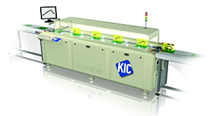
KIC announced that it will exhibit at the SMTA Chihuahua Expo & Tech Forum, scheduled to take place Thursday, March 19, 2020 at the Villarreal Eventos in Chihuahua, CP. Miguel Carbajal, KIC’s Mexico Sales Manager, will discuss the company’s Smart Factory solutions that provide process control, traceability, automation, connectivity, data collection and analytics, and fast and easy integration for i4.0.
Have SPI and AOI but not RPI? Find out what you’re missing without Reflow Process Inspection. With RPI i4.0, and KIC’s NPI and process setup tools, all relevant data can connect to the factory MES or your factory data collection system to be easily analyzed and shared with personnel for clear factory analytics, optimization and corrective action.
Move toward the future of line connectivity, flexible production, machine learning and real-time insight. For more information about KIC, visit www.kicthermal.com.
Share on:


Testimonial
"We’re proud to call I-Connect007 a trusted partner. Their innovative approach and industry insight made our podcast collaboration a success by connecting us with the right audience and delivering real results."
Julia McCaffrey - NCAB GroupSuggested Items
The Art and Science of PCB Floor Planning: A Comprehensive Guide
08/14/2025 | Cory Grunwald and Jeff Reinhold, Monsoon SolutionsPCB design is an intricate and crucial part of developing electronic products. One of the foundational stages of PCB design is floor planning, a phase where the placement of components and the flow of signals are meticulously mapped out. A good floor plan ensures that the PCB performs well, is easy to manufacture, and meets all mechanical and electrical requirements. We’ll explore the essential aspects of floor planning, from its objectives and process to the challenges that designers face.
Advint and SanRex Expand High-Performance DC Rectifier Access for North American PCB Fabricators
08/12/2025 | Advint IncorporatedAdvint Incorporated has entered a strategic partnership with SanRex Corporation, enhancing access to industrial-grade DC rectifiers for the US printed circuit board industry. With a legacy of power innovation and performance across the globe, SanRex rectifiers are available through Advint’s proficient distribution network.
Advint and Sayron Bring Advanced Rectifier Solutions to High-Reliability PCB Manufacturers
08/01/2025 | Advint IncorporatedAdvint Incorporated has partnered with Sayron, a leading global rectifier manufacturer, to supply cutting-edge IGBT-based DC rectifiers to high-performance PCB manufacturers across North America and beyond. Sayron’s precision-engineered rectifiers align with the stringent requirements of advanced PCB processes.
Trouble in Your Tank: Metallizing Flexible Circuit Materials—Mitigating Deposit Stress
08/04/2025 | Michael Carano -- Column: Trouble in Your TankMetallizing materials, such as polyimide used for flexible circuitry and high-reliability multilayer printed wiring boards, provide a significant challenge for process engineers. Conventional electroless copper systems often require pre-treatments with hazardous chemicals or have a small process window to achieve uniform coverage without blistering. It all boils down to enhancing the adhesion of the thin film of electroless copper to these smooth surfaces.
Magnalytix’s Dr. Mike Bixenman to Guide PDC at SMTA High-Reliability Cleaning and Conformal Coating Conference
07/31/2025 | MAGNALYTIXMagnalytix, providing real-time reliability solutions for electronics manufacturing, is excited to announce that Dr. Mike Bixenman will present the professional development course “The Effects of Flux Residues and Process Contamination on the Reliability of the Electronic Assembly” on Wednesday, Aug. 13 at 9:00 AM CST to open the second day of the STMA High-Reliability Cleaning and Conformal Coating Conference.