


 The Marketing Minute: If Your Marketing Budget Gets Cut in Half, Then What?
 Punching Out: How Are the Big Boys in Electronics Doing?
 It’s Only Common Sense: Complexity Is the Enemy of Profit


Integrating Electronics Onto Physical Prototypes
March 4, 2020 | MITEstimated reading time: 4 minutes
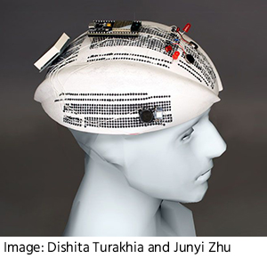
MIT researchers have invented a way to integrate “breadboards” — flat platforms widely used for electronics prototyping — directly onto physical products. The aim is to provide a faster, easier way to test circuit functions and user interactions with products such as smart devices and flexible electronics.
Breadboards are rectangular boards with arrays of pinholes drilled into the surface. Many of the holes have metal connections and contact points between them. Engineers can plug components of electronic systems — from basic circuits to full computer processors — into the pinholes where they want them to connect. Then, they can rapidly test, rearrange, and retest the components as needed.
But breadboards have remained that same shape for decades. For that reason, it’s difficult to test how the electronics will look and feel on, say, wearables and various smart devices. Generally, people will first test circuits on traditional breadboards, then slap them onto a product prototype. If the circuit needs to be modified, it’s back to the breadboard for testing, and so on.
In a paper being presented at CHI (Conference on Human Factors in Computing Systems), the researchers describe “CurveBoards,” 3D-printed objects with the structure and function of a breadboard integrated onto their surfaces. Custom software automatically designs the objects, complete with distributed pinholes that can be filled with conductive silicone to test electronics. The end products are accurate representations of the real thing, but with breadboard surfaces.
CurveBoards “preserve an object’s look and feel,” the researchers write in their paper, while enabling designers to try out component configurations and test interactive scenarios during prototyping iterations. In their work, the researchers printed CurveBoards for smart bracelets and watches, Frisbees, helmets, headphones, a teapot, and a flexible, wearable e-reader.
“On breadboards, you prototype the function of a circuit. But you don’t have context of its form — how the electronics will be used in a real-world prototype environment,” says first author Junyi Zhu, a graduate student in the Computer Science and Artificial Intelligence Laboratory (CSAIL). “Our idea is to fill this gap, and merge form and function testing in very early stage of prototyping an object. … CurveBoards essentially add an additional axis to the existing [three-dimensional] XYZ axes of the object — the ‘function’ axis.”
Joining Zhu on the paper are CSAIL graduate students Lotta-Gili Blumberg, Martin Nisser, and Ethan Levi Carlson; Department of Electrical Engineering and Computer Science (EECS) undergraduate students Jessica Ayeley Quaye and Xin Wen; former EECS undergraduate students Yunyi Zhu and Kevin Shum; and Stefanie Mueller, the X-Window Consortium Career Development Assistant Professor in EECS.
Custom software and hardware
A core component of the CurveBoard is custom design-editing software. Users import a 3D model of an object. Then, they select the command “generate pinholes,” and the software automatically maps all pinholes uniformly across the object. Users then choose automatic or manual layouts for connectivity channels. The automatic option lets users explore a different layout of connections across all pinholes with the click of a button. For manual layouts, interactive tools can be used to select groups of pinholes and indicate the type of connection between them. The final design is exported to a file for 3D printing.
When a 3D object is uploaded, the software essentially forces its shape into a “quadmesh” — where the object is represented as a bunch of small squares, each with individual parameters. In doing so, it creates a fixed spacing between the squares. Pinholes — which are cones, with the wide end on the surface and tapering down — will be placed at each point where the corners of the squares touch. For channel layouts, some geometric techniques ensure the chosen channels will connect the desired electrical components without crossing over one another.
In their work, the researchers 3D printed objects using a flexible, durable, nonconductive silicone. To provide connectivity channels, they created a custom conductive silicone that can be syringed into the pinholes and then flows through the channels after printing. The silicone is a mixture of a silicone materials designed to have minimal electricity resistance, allowing various types electronics to function.
To validate the CurveBoards, the researchers printed a variety of smart products. Headphones, for instance, came equipped with menu controls for speakers and music-streaming capabilities. An interactive bracelet included a digital display, LED, and photoresistor for heart-rate monitoring, and a step-counting sensor. A teapot included a small camera to track the tea’s color, as well as colored lights on the handle to indicate hot and cold areas. They also printed a wearable e-book reader with a flexible display.
Better, faster prototyping
In a user study, the team investigated the benefits of CurveBoards prototyping. They split six participants with varying prototyping experience into two sections: One used traditional breadboards and a 3D-printed object, and the other used only a CurveBoard of the object. Both sections designed the same prototype but switched back and forth between sections after completing designated tasks. In the end, five of six of the participants preferred prototyping with the CurveBoard. Feedback indicated the CurveBoards were overall faster and easier to work with.
But CurveBoards are not designed to replace breadboards, the researchers say. Instead, they’d work particularly well as a so-called “midfidelity” step in the prototyping timeline, meaning between initial breadboard testing and the final product. “People love breadboards, and there are cases where they’re fine to use,” Zhu says. “This is for when you have an idea of the final object and want to see, say, how people interact with the product. It’s easier to have a CurveBoard instead of circuits stacked on top of a physical object.”
Next, the researchers hope to design general templates of common objects, such as hats and bracelets. Right now, a new CurveBoard must built for each new object. Ready-made templates, however, would let designers quickly experiment with basic circuits and user interaction, before designing their specific CurveBoard.
Additionally, the researchers want to move some early-stage prototyping steps entirely to the software side. The idea is that people can design and test circuits — and possibly user interaction — entirely on the 3D model generated by the software. After many iterations, they can 3D print a more finalized CurveBoard. “That way you’ll know exactly how it’ll work in the real world, enabling fast prototyping,” Zhu says. “That would be a more ‘high-fidelity’ step for prototyping.”
Share on:


Testimonial
"Our marketing partnership with I-Connect007 is already delivering. Just a day after our press release went live, we received a direct inquiry about our updated products!"
Rachael Temple - AlltematedSuggested Items
BAE Systems Provides Advanced Aircraft Readiness with New Link 16 Test Capability for F-16
05/14/2026 | BAE SystemsBAE Systems has completed the successful development and integration of an upgraded Link 16 test capability for Multifunctional Information Distribution System Joint Tactical Radio System (MIDS JTRS) terminals on U.S. Air Force F-16 aircraft.
Separating Fact from Fear on the FCC ‘China Lab Ban’
05/14/2026 | Jan Pedersen, NCAB GroupRecent news headlines have suggested that the U.S. Federal Communications Commission (FCC) has “banned all testing laboratories in China and Hong Kong.” Understandably, this has created concerns around PCB testing, material approvals, UL listings, and the continued use of established test laboratories in Asia. The good news is that for most PCB, PCB material, and PCBA testing, nothing has changed. Let’s separate fact from fear.
yieldWerx, WATS Partner to Bridge PCB Test with Chip-Level Manufacturing Data
05/11/2026 | PRNewswireBoard-level and semiconductor test data are often analyzed separately, limiting correlation across the product lifecycle. Linking PCB assembly (PCBA) test results, including in-circuit and functional test, with upstream wafer, sort, and final test data remains difficult, particularly in photonics, advanced packaging, and high-density integration environments.
SPEA Expands Global Footprint with New Hub in Santa Clara, Silicon Valley
05/08/2026 | SPEASPEA has officially landed in the heart of Silicon Valley, with the grand opening of its newest facility in Santa Clara, California.
More Than Electrical Test: TTCI to Spotlight X-ray and CT Capabilities at SMTA Capital Expo
05/07/2026 | TTCIThe Training Connection LLC (TTC-LLC) will exhibit at the SMTA Capital Expo on Thursday, May 14 at the DoubleTree by Hilton Baltimore - BWI Airport.