-
- News
- Books
Featured Books
- design007 Magazine
Latest Issues
Current IssueSignal Integrity
If you don’t have signal integrity problems now, you will eventually. This month, our expert contributors share a variety of SI techniques that can help designers avoid ground bounce, crosstalk, parasitic issues, and much more.
Proper Floor Planning
Floor planning decisions can make or break performance, manufacturability, and timelines. This month’s contributors weigh in with their best practices for proper floor planning and specific strategies to get it right.
Showing Some Constraint
A strong design constraint strategy carefully balances a wide range of electrical and manufacturing trade-offs. This month, we explore the key requirements, common challenges, and best practices behind building an effective constraint strategy.
- Articles
- Columns
- Links
- Media kit
||| MENU - design007 Magazine
Ventec High Performance IMS Dielectric Material VT-4B5H Receives UL-Authorization
April 29, 2020 | Ventec International Group Co., Ltd.Estimated reading time: 2 minutes

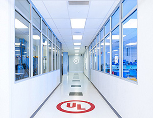
Ventec International Group Co., Ltd., is pleased to announce that UL’s evaluation of Ventec’s high-performance ceramic-filled, non-reinforced IMS dielectric material has received authorization to apply the UL mark and has thus been recognized for achieving 155°C maximum operating temperature (MOT) for electric and mechanical RTI (Relative Temperature Index).
UL's investigation of Ventec's VT-4B5H metal base laminate has been completed and was determined to comply with the applicable requirements including 155oC MOT (maximum operating temperature) for electric and mechanical RTI (Relative Temperature Index). With thermal conductivity of 4.2 W/m*K and glass transition temperature (Tg) of 180°C, the versatile IMS material is the perfect choice for use in extreme high temperature applications. These include DC/DC power modules, IGBT applications, motor controllers, high lumen output LED devices, battery charging, OBC chargers for EV vehicles and several other automotive “underhood” applications. VT-4B5H is also highly recommended for chip on board (COB) or direct die in both power and LED applications.
VT-4B5H is available in a wide range of dielectric-, copper foil- and base plate thicknesses and types as well as in numerous panel size options. This versatility is ideal for both single layer and multiple layer IMS designs.
Chris Hanson, Global Head IMS Technology, commented: "Achieving UL authorization for VT-4B5H’s industry-leading 155°C MOT performance is fantastic news. As a complement to our full VT-4B series of superior thermal dissipation materials, our customers have access to an IMS material that meets virtually any high thermal performance requirements."
Ventec International is a world leader in the production of polyimide and high reliability epoxy laminates and prepregs and specialist provider of thermal management and IMS solutions. Further information about Ventec’s solutions and the company’s wide variety of products is available at www.venteclaminates.com and/or by downloading the Ventec APP.
About Ventec International Group
Ventec International is a premier supplier to the Global PCB industry. With volume manufacturing facilities in Taiwan and China and distribution locations and manufacturing sites in both the US and Europe, Ventec specializes in advanced copper-clad glass-reinforced and metal-backed substrates. Ventec materials, which include high-quality enhanced FR-4, high-speed/low-loss- and high-performance IMS material technology and an advanced range of thermal management solutions, are manufactured by Ventec using strict quality-controlled processes that are certified to AS9100 Revision D, IATF 16949:2016 and ISO 9001:2015, and are backed by a fully controlled and managed global supply chain, sales- and technical support-network.
For more information, visit www.venteclaminates.com.
Testimonial
"We’re proud to call I-Connect007 a trusted partner. Their innovative approach and industry insight made our podcast collaboration a success by connecting us with the right audience and delivering real results."
Julia McCaffrey - NCAB GroupSuggested Items
Trouble in Your Tank: Implementing Direct Metallization in Advanced Substrate Packaging
09/15/2025 | Michael Carano -- Column: Trouble in Your TankDirect metallization systems based on conductive graphite are gaining popularity throughout the world. The environmental and productivity gains achievable with this process are outstanding. Direct metallization reduces the costs of compliance, waste treatment, and legal issues related to chemical exposure. A graphite-based direct plate system has been devised to address these needs.
Closing the Loop on PCB Etching Waste
09/09/2025 | Shawn Stone, IECAs the PCB industry continues its push toward greener, more cost-efficient operations, Sigma Engineering’s Mecer System offers a comprehensive solution to two of the industry’s most persistent pain points: etchant consumption and rinse water waste. Designed as a modular, fully automated platform, the Mecer System regenerates spent copper etchants—both alkaline and acidic—and simultaneously recycles rinse water, transforming a traditionally linear chemical process into a closed-loop system.
Driving Innovation: Depth Routing Processes—Achieving Unparalleled Precision in Complex PCBs
09/08/2025 | Kurt Palmer -- Column: Driving InnovationIn PCB manufacturing, the demand for increasingly complex and miniaturized designs continually pushes the boundaries of traditional fabrication methods, including depth routing. Success in these applications demands not only on robust machinery but also sophisticated control functions. PCB manufacturers rely on advanced machine features and process methodologies to meet their precise depth routing goals. Here, I’ll explore some crucial functions that empower manufacturers to master complex depth routing challenges.
Trouble in Your Tank: Minimizing Small-via Defects for High-reliability PCBs
08/27/2025 | Michael Carano -- Column: Trouble in Your TankTo quote the comedian Stephen Wright, “If at first you don’t succeed, then skydiving is not for you.” That can be the battle cry when you find that only small-diameter vias are exhibiting voids. Why are small holes more prone to voids than larger vias when processed through electroless copper? There are several reasons.
The Government Circuit: Navigating New Trade Headwinds and New Partnerships
08/25/2025 | Chris Mitchell -- Column: The Government CircuitAs global trade winds continue to howl, the electronics manufacturing industry finds itself at a critical juncture. After months of warnings, the U.S. Government has implemented a broad array of tariff increases, with fresh duties hitting copper-based products, semiconductors, and imports from many nations. On the positive side, tentative trade agreements with Europe, China, Japan, and other nations are providing at least some clarity and counterbalance.