-

- News
- Books
Featured Books
- design007 Magazine
Latest Issues
Current Issue
Designing Proper Work-Life Balance
In this issue, we hear from designers, marketers, and business owners on how they apply their professional skills to their personal lives to build a healthier work-life balance.

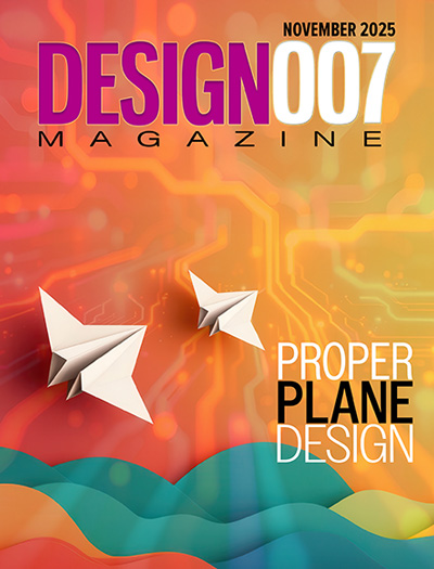
Designing Proper Planes
Without planes, designers would have to create thousands of traces to accomplish the same objectives. Power planes provide low impedance and stable power, and ground planes stabilize reference voltage, improve thermal performance, and help preclude EMI issues.

Power Integrity
Current power demands are increasing, especially with AI, 5G, and EV chips. This month, our experts share “watt’s up” with power integrity, from planning and layout through measurement and manufacturing.
- Articles
- Columns
- Links
- Media kit
||| MENU - design007 Magazine
Zuken Reduces Wire Harness Time to Manufacture
May 18, 2020 | ZukenEstimated reading time: 2 minutes
Harness Builder 2020 for E3.series has been enhanced to provide extended control and processing capabilities for wire harness manufacturers.
Harness Builder for E3.series is a packaged solution that allows harness manufacturers to generate accurate customer quotations. From there, the underlying design database can be reused – not reinvented – to create the manufacturable formboard design, saving time and maintaining the accuracy of the design.
“We’re edging closer to the perfect solution for creating wire harness quotations faster and more accurately, while providing the functionality to enter the manufacturing stage much earlier by using the same tool for both jobs,” says Paul Harvell, Product Director of E3.series.
Auto-placement of device and cable labels
Auto-placement of device and cable labels, along with heat shrinks, substantially decreases the tedious job of manual measurement and placement on the harness drawing. Labels are dynamically selected based on wire bundle size and auto-placed on connector ends or on the complete harness. The label data becomes part of the system and can be printed locally or sent to industrial label printing machines during the harness assembly process.
User-definable content is extracted directly from the design for printing or exported to vital build documentation eliminating the need to check for compatibility and accuracy of the information against the design.
The new release features auto-placement of tape and/or fixings in predefined positions on nets and set distances from connector ends. Tape, labels, and heat shrinks are automatically added to the quotation and the bills of materials if required.
Drafting co-pilot
Harness Builder 2020 for E3.series includes a new drafting co-pilot that allows the user to enter predefined wire or cable lengths. Now a fixed length cable can be wound around a pin or peg on the formboard, maintaining the predefined length without requiring orthogonal placement. This means a much smaller formboard can be used for building the harness, occupying less space on the manufacturing floor.
Support for third-party test and manufacturing equipment
Support for third-party test and manufacturing exports has been expanded. Harnesses created with Harness Builder 2020 for E3.series can now be exported directly to CableScan for testing. This integration adds to our growing list of supported vendors that includes Cami Research, Cirris, DIT-MCO, and Dynalab.
Also included in the 2020 release is a new export utility to drive the ProjectionWorks (a division of Delta Sigma) family of manufacturing equipment. Harness placement and wiring information is exported from the Zuken tool and projected directly on the formboard as augmented reality work instructions. This combined solution reduces manual errors and speeds time to manufacture.
Cable tolerancing
Based on feedback from the military sector, Harness Builder 2020 for E3.series now adheres to the user-driven tolerancing on the drawing sheet to influence the cable lengths. When setting cable tolerancing, this new feature provides the user with a sliding scale of tolerancing based on the length and complexity of the cables, improving the overall build accuracy.
Harness Builder 2020 for E3.series is available now in North America.
Testimonial
"In a year when every marketing dollar mattered, I chose to keep I-Connect007 in our 2025 plan. Their commitment to high-quality, insightful content aligns with Koh Young’s values and helps readers navigate a changing industry. "
Brent Fischthal - Koh YoungSuggested Items
Libra Industries Names Tony Jepson as General Manager of Dallas Facility
01/15/2026 | Libra IndustriesLibra Industries, a leading provider of systems integration and electronics manufacturing services (EMS), is proud to announce the appointment of Tony Jepson as the new General Manager of its Dallas, Texas facility.
Absolute EMS Forms Strategic Partnership with Global Manufacturing Leader SIIX USA
01/15/2026 | Absolute EMS, Inc.Absolute EMS, Inc., a six-time award-winning provider of fast turnaround, turnkey contract electronic manufacturing services (EMS), is pleased to announce that it has entered into a strategic contractual agreement with SIIX USA, a Japan-headquartered global manufacturing and trading firm.
Technica USA Named Exclusive U.S. Distributor for Wise in the State of Texas
01/15/2026 | Technica USATechnica USA is proud to announce the expansion of their distribution rights with Wise s.r.l. Parma Italy into the State of Texas, effective January 1, 2026
Siemens Acquires ASTER Technologies to Deliver Industry-leading PCB Test Engineering Solutions
01/14/2026 | PRNewswireSiemens announced it has acquired ASTER Technologies ("ASTER"), a privately held market leader in printed circuit board assembly (PCBA) test verification and engineering software.
Kimball Electronics Sets Ribbon-Cutting for New Indianapolis Medical Facility
01/13/2026 | Kimball ElectronicsKimball Electronics, Inc. announced the date for the ribbon-cutting ceremony at its new medical manufacturing facility in Indianapolis.


