


 Fresh PCB Concepts: Resilience and Renewal in Domestic PCB Manufacturing
 Designers Notebook: Power and Ground Distribution Basics
 Elementary, Mr. Watson: Heat—The Hidden Villain of Power Electronics


Pasternack Launches Seven New Fixed Load VNA Calibration Kits
June 1, 2020 | PasternackEstimated reading time: 1 minute
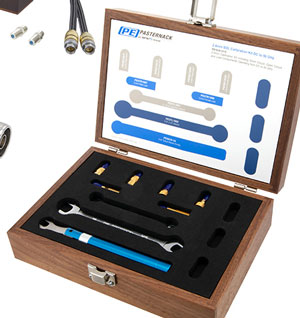
Pasternack, an Infinite Electronics brand and a leading provider of RF, microwave and millimeter wave products, has just released a new line of short-open-load-through (SOLT) calibration kits that are ideal for use in test and measurement, lab and RF & Microwave production test applications.
Pasternack’s expanded line of VNA calibration kits are available in 12 versions including short circuit, open circuit and load kits (SOL) as well as short circuit, open circuit, load and thru kits (SOLT) with 2.4mm, 2.92mm, 3.5mm, 7/16 DIN, 7mm, BNC and N-Type interface options.
Each of these new VNA calibration kits from Pasternack include all of the necessary short circuit, open circuit, loads and thru (model dependent) components required for VNA calibration. The kits are suitable for many vector network analyzers from the industry’s leading providers such as Agilent, Rohde & Schwarz, Anritsu and Copper Mountain. These RF test and measurement kits come packaged in protective wooden boxes.
The new SOLT calibration kits offer excellent performance characteristics that are specially designed for the fine-tuning and calibration of sensitive test equipment in engineering labs, production environments and quality testing facilities. Every Pasternack calibration kit is built to withstand years of rigorous use and provides accurate RF equipment calibration for the life of the product.
“A properly calibrated VNA is required for precise characterization of RF and microwave components used in a myriad of industries and applications. These new SOLT calibration kits provide the precision components that are essential to perform accurate analyzer calibrations,” said Steve Ellis, Interconnect Product Line Manager at Pasternack.
Share on:


Testimonial
"The I-Connect007 team is outstanding—kind, responsive, and a true marketing partner. Their design team created fresh, eye-catching ads, and their editorial support polished our content to let our brand shine. Thank you all! "
Sweeney Ng - CEE PCBSuggested Items
WestDev Announces Advanced Thermal Analysis Integration for Pulsonix PCB Design Suite
10/29/2025 | WestDev Ltd.Pulsonix, the industry-leading PCB design software from WestDev Ltd., announced a major enhancement to its design ecosystem: a direct interface between Pulsonix and ADAM Research's TRM (Thermal Risk Management) analysis software.
Designers Notebook: Power and Ground Distribution Basics
10/29/2025 | Vern Solberg -- Column: Designer's NotebookThe principal objectives to be established during the planning stage are to define the interrelationship between all component elements and confirm that there is sufficient surface area for placement, the space needed to ensure efficient circuit interconnect, and to accommodate adequate power and ground distribution.
Episode 6 of Ultra HDI Podcast Series Explores Copper-filled Microvias in Advanced PCB Design and Fabrication
10/15/2025 | I-Connect007I-Connect007 has released Episode 6 of its acclaimed On the Line with... American Standard Circuits: Ultra High Density Interconnect (UHDI) podcast series. In this episode, “Copper Filling of Vias,” host Nolan Johnson once again welcomes John Johnson, Director of Quality and Advanced Technology at American Standard Circuits, for a deep dive into the pros and cons of copper plating microvias—from both the fabricator’s and designer’s perspectives.
Nolan’s Notes: Tariffs, Technologies, and Optimization
10/01/2025 | Nolan Johnson -- Column: Nolan's NotesLast month, SMT007 Magazine spotlighted India, and boy, did we pick a good time to do so. Tariff and trade news involving India was breaking like a storm surge. The U.S. tariffs shifted India from one of the most favorable trade agreements to the least favorable. Electronics continue to be exempt for the time being, but lest you think that we’re free and clear because we manufacture electronics, steel and aluminum are specifically called out at the 50% tariff levels.
MacDermid Alpha & Graphic PLC Lead UK’s First Horizontal Electroless Copper Installation
09/30/2025 | MacDermid Alpha & Graphic PLCMacDermid Alpha Electronics Solutions, a leading supplier of integrated materials and chemistries to the electronics industry, is proud to support Graphic PLC, a Somacis company, with the installation of the first horizontal electroless copper metallization process in the UK.