


 The Marketing Minute: If Your Marketing Budget Gets Cut in Half, Then What?
 Punching Out: How Are the Big Boys in Electronics Doing?
 It’s Only Common Sense: Complexity Is the Enemy of Profit


Project HiperLAM Delivers Outstanding Results Using PV Nano Cell’s Sicrys Ink
June 17, 2020 | PV Nano CellEstimated reading time: 2 minutes
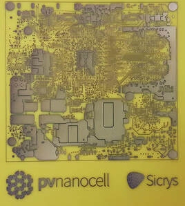
PV Nano Cell Ltd, an innovative provider of inkjet-based conductive digital printing solutions and producer of conductive digital inks, announced that its Sicrys™ ink was successfully used to deliver exceptional results in HiperLAM—a European Union-funded program to laser print RFID antennas and fingerprint sensors.
The HiperLAM project is focused on demonstrating superior cost and speed performance in end-to-end processes featuring laser-based additive manufacturing. Two key applications requiring high resolution printed conductive metallic lines are studied. Laser printed RFID antennas and laser printed fingerprint sensors. The project received funding from the European Union's Horizon 2020 Research and Innovation Program under Grant Agreement No. 723879.
PV Nano Cell’s Chief Executive Officer, Dr. Fernando de la Vega, commented, “We are happy to yet again join hands with some of the leading researchers and commercial companies in the world to develop new digital additive manufacturing technologies. This time we focus on LIFT – Laser Induced Forward Transfer technology. This technology enables printing in both solid and liquid phase, down to 10 µm in resolution, a variety of materials are supported and no use of nozzles. We provided our specially designed ink to accommodate the unique needs of the technology and I'm happy to share the results were very impressive. The lines width achieved is around 90 µm and the pitch is around 20 µm. The printed samples are of excellent quality, with low resistance and suitable for high frequency band applications.”
One of the leading partners in this program is NTUA - National Technical University of Athens. Professor Ioanna Zergioti from the School of Applied Mathematics and Physical Sciences commented, “Our collaboration with PV Nano Cell (PVN) resulted in new scientific results but also in new products. This combination is very difficult to achieve and we thank the team from PVN for their contribution to deliver high quality work and producing new inks for the digital printing process.”
PV Nano Cell’s Chief of Business Development Officer, Mr. Hanan Markovich commented, “Demonstrating commercial capabilities of the LIFT technology is of high importance to PV Nano Cell as we develop additional additive manufacturing products for conductive printing. We believe there is great potential in using lasers to print and that this technology is complementary to inkjet printing. We've already started to formulate new partnerships in this area and look forward to growing the business with yet another, new and exciting potential growth engine.”
Share on:


Testimonial
"In a year when every marketing dollar mattered, I chose to keep I-Connect007 in our 2025 plan. Their commitment to high-quality, insightful content aligns with Koh Young’s values and helps readers navigate a changing industry. "
Brent Fischthal - Koh YoungSuggested Items
Absolute EMS Expands Support for LEO, MEO, and GEO Satellite Programs
05/13/2026 | Absolute EMS, Inc.Absolute EMS, Inc., a Silicon Valley–based provider of high-technology electronics manufacturing services, continues to grow its presence in the satellite sector, supporting programs across low Earth orbit (LEO), medium Earth orbit (MEO), and geostationary orbit (GEO) with advanced PCBA manufacturing, test, and sub-assembly capabilities.
Advance Your Electronics Expertise in June and July
05/14/2026 | Global Electronics AssociationStay current with design, manufacturing, and quality standards by enrolling in one of these online instructor-led courses starting in June and July from ElectronicsU at the Global Electronics Association, designed to help professionals at every level sharpen their skills and advance their careers. These live, expert-led sessions combine flexibility with real-time interaction, allowing participants to learn directly from seasoned industry professionals while collaborating with peers worldwide. Access to all applicable IPC standards is included in the courses.
Road to Reliability: Engineering High Uptime EV Charging Infrastructure
05/13/2026 | Stanton Rak, SF Rak CompanyThe transition to EVs is no longer constrained solely by vehicle capability. Instead, it is increasingly defined by a simpler, but more unforgiving question: Will the charger work when I arrive? This high uptime does not happen by accident. As EV technology has matured, limitations in battery range, power electronics, and thermal management are no longer the primary barriers to adoption.
Intel Foundry Push Gains Momentum With Apple as Potential Customer
05/13/2026 | I-Connect007 Editorial TeamApple’s reported decision to tap Intel as a manufacturing partner for future chips could mark one of the most significant shifts in the semiconductor supply chain in years, with implications that extend well beyond consumer electronics.
Scanfil Signs Agreement with Leading Industrial Automation Company
05/13/2026 | ScanfilScanfil has signed an agreement with a leading industrial automation company, part of a global technology group, strengthening its position in demanding industrial automation and electronics manufacturing applications.