


 The Marketing Minute: If Your Marketing Budget Gets Cut in Half, Then What?
 Punching Out: How Are the Big Boys in Electronics Doing?
 It’s Only Common Sense: Complexity Is the Enemy of Profit


PV Nano Cell Introduces 7 New Digital Conductive Inks
December 14, 2020 | Globe NewswireEstimated reading time: 2 minutes
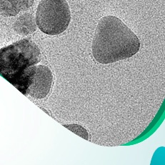
PV Nano Cell Ltd., an innovative provider of inkjet-based conductive digital printing solutions and producer of conductive digital inks, has announced that it is introducing additional digital conductive inks meant for Solar, Ceramic, Glass, LIFT and Generic Applications. The newly introduced inks are meant for the following digital conductive printing technologies: inkjet, aerosol and Laser Induced Forward Transfer.
PV Nano Cell is introducing and making public a total of 7 new digital conductive inks. 2 silver conductive inks for general purpose applications, 2 silver conductive inks with glass frits for solar, ceramic and glass application, 2 copper conductive inks and 1 new copper-based high-viscous ink for LIFT printing. The new inks cover a range of metal loads from 20% to 60% silver or copper, various solvents and optimization to conductive printing technologies including inkjet, aerosol and LIFT.
PV Nano Cell’s Chief Executive Officer, Dr. Fernando de la Vega, commented, “These newly introduced inks are the result of market and customers' requirements that we see growing over the past year. First, in the glass-related industry we see many new applications and use cases emerging for automotive, such as the case with project Tinker we released a PR about most recently. Second, solar-related customers of ours are realizing the phenomenal advantage of using our complete solution in dramatically increasing their overall power efficiency. Last and not least we experience strong demand for additional inks to support a wide array of IoT applications, including sensors, antennas, PCB and medical-related. The ability to introduce new conductive inks heavily relies on our strong IP and patents relating to our Sicrys™ conductive silver and coper inks. This IP allows us to quickly and efficiently respond to market needs and develop and optimize new ink products for our customers.”
PV Nano Cell’s Chief of Business Development Officer, Mr. Hanan Markovich commented, “Our complete solution approach of conductive inks, printers and printing process, naturally leverages our conductive ink technology advantages. Alongside our off the shelf products we are requested to either optimize or develop new inks per specific customer requirements. Our core chemistry competency enables us to fully control properties such as the type of metal, metal load, type of solvent, viscosity, printing technology designation and even the size of the nano-particles. By balancing these properties, we are able to carefully craft superior performing inks to be used in mass-production applications with high-throughput printing. Some of the new ink technologies developed we modify for more general purposes that can be used by many of our customers. These new inks will support the further growth of our business in mass-production applications.”
As most recently published, PV Nano Cell announced that the European Union ?s H2020 funded TINKER project in which the Company is a partner, has started. TINKER is set to develop a new reliable, cost-and resource efficient pathway for automotive RADAR and LiDAR sensor package fabrication based on additive manufacturing.
Share on:


Testimonial
"Your magazines are a great platform for people to exchange knowledge. Thank you for the work that you do."
Simon Khesin - Schmoll MaschinenSuggested Items
I-Connect007 Releases The Printed Circuit Designer’s Guide to… Direct Metallization: A Guide to Complex PCB Fabrication
05/13/2026 | I-Connect007As PCB complexity continues to accelerate, fabricators and OEMs are reevaluating long-standing manufacturing processes to meet the demands of AI, HDI, advanced packaging, and next-generation electronics. To address these evolving challenges, I-Connect007 is proud to announce the release of The Printed Circuit Designer’s Guide to… Direct Metallization: A Guide to Complex PCB Fabrication, authored by MacDermid Alpha Solution’s Carmichael Gugliotti.
Driving Innovation: Selecting the Right Laser Source
04/28/2026 | Simon Khesin -- Column: Driving InnovationWhen I first joined Schmoll Maschinen, I brought experience from almost every PCB process, except for laser. As I immersed myself in laser processing, I realized why it can seem so daunting to a newcomer. The complexity arises from three intersecting factors: A vast variety of laser sources: CO2, UV-nano, green-pico, UV-pico, IR-pico, and others; a diverse range of applications: Drilling, cutting, ablation, and more; and an extensive list of materials: These have vastly different absorption rates. Choosing the right machine or laser source is rarely trivial. Even for experienced engineers, answering "Which source is best?" requires examining the business's specific goals.
Institute of Circuit Technology Spring Seminar 2026: A Bright Future in Europe
04/23/2026 | Pete Starkey, I-Connect007Through the leafy lanes and spring flowers of Warwickshire and back to Meridan, the traditional centre of England, and now officially part of the Metropolitan Borough of Solihull in the county of the West Midlands, I attended the Annual General Meeting and Spring Seminar of the Institute of Circuit Technology (ICT) on April 14. Out of the AGM came notable changes in leadership at the top of the Institute: the retirement of Mat Beadel as chair and Emma Hudson as technical director. Effective May 1, Steve Driver is the new chair, and Alun Morgan is the new technical director.
ACCM Unveils Negative and Near-zero CTE Materials for Large-Format AI Chips
04/21/2026 | Advanced Chip and Circuit MaterialsAdvanced Chip and Circuit Materials, Inc. (ACCM) has launched two new materials: Celeritas HM50, with a negative coefficient of thermal expansion (CTE) of -8 ppm/°C to offset the positive CTE and expansion of copper with temperature on circuit boards, and Celeritas HM001, with near-zero CTE and the low-loss performance needed for high-speed signal layers to 224 Gb/s and faster in artificial intelligence (AI) circuits.
Fresh PCB Concepts: Designing PCBs for Harsh Environments—Reliability Is Engineered Upstream
04/23/2026 | Team NCAB -- Column: Fresh PCB ConceptsWhen engineers hear the phrase “harsh environment,” they usually think of the extreme temperature swings, vibration and shock, pressure changes, or radiation in aerospace. However, aerospace is not the only harsh environment where electronic assemblies must survive. Automotive power electronics, downhole oil and gas tools, marine controls, rail systems, defense platforms, and industrial automation equipment all expose PCBs to environments that are equally unforgiving. The stress mechanisms may differ, but the physics does not.