-
- News
- Books
Featured Books
- I-Connect007 Magazine
Latest Issues
Current Issue
Beyond the Rulebook
What happens when the rule book is no longer useful, or worse, was never written in the first place? In today’s fast-moving electronics landscape, we’re increasingly asked to design and build what has no precedent, no proven path, and no tidy checklist to follow. This is where “Design for Invention” begins.
March Madness
From the growing role of AI in design tools to the challenge of managing cumulative tolerances, these articles in this issue examine the technical details, design choices, and manufacturing considerations that determine whether a board works as intended.
Looking Forward to APEX EXPO 2026
I-Connect007 Magazine previews APEX EXPO 2026, covering everything from the show floor to the technical conference. For PCB designers, we move past the dreaded auto-router and spotlight AI design tools that actually matter.
- Articles
- Columns
- Links
- Media kit
||| MENU - I-Connect007 Magazine
Ventec, BizLink, Footprintku Announce Strategic Alliance
February 26, 2021 | VentecEstimated reading time: 2 minutes
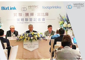
Ventec is pleased to announce that it has entered into a global strategic alliance with leading interconnect solutions provider, BizLink Holding Inc., and Footprintku Inc., an online EDA library and digital transformation services provider for electronic components. This alliance is formed to provide a solution that boosts product development process efficiency and shortens development and time-to-market.
BizLink has long been a supplier of key components to the IT industry, including connectors and cables. The company is experienced in new product introduction (NPI) as well as in system integration, manufacturing, and in assembly.
BizLink’s Chairman, Roger Liang, said, "For the design of electronic products, the trend is for thinner, lighter, and aesthetically pleasing products whilst maintaining functionality and compatibility. This has prompted the demand for rapid and frequent updates of components and product styles. The ability to quickly develop products to respond to market changes has become the key to success."
Ventec International’s Chairman, Tony Lau, pointed out, "What the market needs is a platform that integrates the advantages of upstream components, mid-section design, and back-end manufacturing. The creation of such a platform, we knew, would greatly help accelerate industrial innovation." Footprintku Inc.’s Chairman, YC Hwang, continued, "In response, we propose a cloud platform using the exclusive AI and digital transformation technology of Footprintku.com to integrate the resources of all three companies. The result is a one-stop service, making it possible for product developers to quickly and efficiently find the best components and quality suppliers for their product R&D and design change stages."
This alliance is built upon Footprintku’s cloud database for electronic components as well as BizLink’s solutions and Ventec International’s materials. It integrates the capabilities of new product introduction (NPI), design services (ODM), and manufacturing assembly (EMS). This alliance will reduce the cost of and time in searching for electronic components for product developers. Furthermore, it will accelerate product evolution and facilitate industrial innovation by connecting highly flexible and customized electronic industry supply chain partners.
The alliance was officially announced at a press conference held at the Grand Hyatt Taipei on February 26, 2021.
Testimonial
"Your magazines are a great platform for people to exchange knowledge. Thank you for the work that you do."
Simon Khesin - Schmoll MaschinenSuggested Items
Driving Innovation: Selecting the Right Laser Source
04/28/2026 | Simon Khesin -- Column: Driving InnovationWhen I first joined Schmoll Maschinen, I brought experience from almost every PCB process, except for laser. As I immersed myself in laser processing, I realized why it can seem so daunting to a newcomer. The complexity arises from three intersecting factors: A vast variety of laser sources: CO2, UV-nano, green-pico, UV-pico, IR-pico, and others; a diverse range of applications: Drilling, cutting, ablation, and more; and an extensive list of materials: These have vastly different absorption rates. Choosing the right machine or laser source is rarely trivial. Even for experienced engineers, answering "Which source is best?" requires examining the business's specific goals.
Institute of Circuit Technology Spring Seminar 2026: A Bright Future in Europe
04/23/2026 | Pete Starkey, I-Connect007Through the leafy lanes and spring flowers of Warwickshire and back to Meridan, the traditional centre of England, and now officially part of the Metropolitan Borough of Solihull in the county of the West Midlands, I attended the Annual General Meeting and Spring Seminar of the Institute of Circuit Technology (ICT) on April 14. Out of the AGM came notable changes in leadership at the top of the Institute: the retirement of Mat Beadel as chair and Emma Hudson as technical director. Effective May 1, Steve Driver is the new chair, and Alun Morgan is the new technical director.
ACCM Unveils Negative and Near-zero CTE Materials for Large-Format AI Chips
04/21/2026 | Advanced Chip and Circuit MaterialsAdvanced Chip and Circuit Materials, Inc. (ACCM) has launched two new materials: Celeritas HM50, with a negative coefficient of thermal expansion (CTE) of -8 ppm/°C to offset the positive CTE and expansion of copper with temperature on circuit boards, and Celeritas HM001, with near-zero CTE and the low-loss performance needed for high-speed signal layers to 224 Gb/s and faster in artificial intelligence (AI) circuits.
Fresh PCB Concepts: Designing PCBs for Harsh Environments—Reliability Is Engineered Upstream
04/23/2026 | Team NCAB -- Column: Fresh PCB ConceptsWhen engineers hear the phrase “harsh environment,” they usually think of the extreme temperature swings, vibration and shock, pressure changes, or radiation in aerospace. However, aerospace is not the only harsh environment where electronic assemblies must survive. Automotive power electronics, downhole oil and gas tools, marine controls, rail systems, defense platforms, and industrial automation equipment all expose PCBs to environments that are equally unforgiving. The stress mechanisms may differ, but the physics does not.
Advanced Packaging for AI: Reliability Starts at the Cu/Cu/Cu Microvia Junction
04/20/2026 | Kuldip Johal, MKS' AtotechThe rapid growth of AI computing, from training clusters to inference at scale, is reshaping demand across the entire electronics supply chain. Advances in technology requirements, such as higher bandwidth, lower latency, and greater compute density, are driving the development of advanced packaging technologies and transforming the PCB industry across design, manufacturing, testing, and even architecture.