-

- News
- Books
Featured Books
- design007 Magazine
Latest Issues
Current Issue
Signal Integrity
If you don’t have signal integrity problems now, you will eventually. This month, our expert contributors share a variety of SI techniques that can help designers avoid ground bounce, crosstalk, parasitic issues, and much more.

Proper Floor Planning
Floor planning decisions can make or break performance, manufacturability, and timelines. This month’s contributors weigh in with their best practices for proper floor planning and specific strategies to get it right.

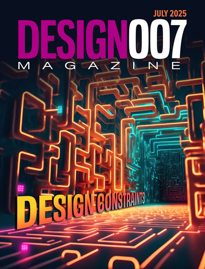
Showing Some Constraint
A strong design constraint strategy carefully balances a wide range of electrical and manufacturing trade-offs. This month, we explore the key requirements, common challenges, and best practices behind building an effective constraint strategy.
- Articles
- Columns
- Links
- Media kit
||| MENU - design007 Magazine
The Art of Using Symmetry—and Asymmetry—in PCB Design
January 6, 2022 | Chris Young, The Goebel CompanyEstimated reading time: 1 minute
An empty board outline is a PCB designer’s empty canvas. Components are the designer’s paint palette, and the traces are the brush strokes used to blend and mesh the components together on the canvas. The subject matter is defined by the schematic entry and the tone is often set according to the purpose of the design. The subject matter’s form emerges during placement and takes shape when routed. The aesthetic nature of a PCB or PCBA is typically judged by the designer’s use of symmetry, focal points, and centers of interest.
The enjoyment experienced by observing a bee (a bilaterally symmetric insect) symbiotically interact with a flower (a radially symmetric plant) is derived from the realization of two well-proportioned beings striking a mutually equitable existence, a classic win-win scenario. I surmise that our use of symmetry in our own creations is our sincerest form of flattery to these well-balanced relationships. Hence, we have embedded symmetry in nearly all aspects of our lives—from our homes, roads, and bridges, right down to the printed circuit board designs present in our modern-day electronics.
We are hard wired to identify symmetry, we tend to find it appealing, and the subject of PCB design is no exception. Symmetry in PCB design is aesthetically pleasing to look at, and the physical balance of components, traces, and layers convey deeper meanings to the observer.
Further observation will reveal that this board design is the physical representation of two identical circuits running vertically and each circuit is composed of two sub-sections distinctly spaced apart horizontally.
These PCBs and circuit boards that exhibit symmetry are typically easier to troubleshoot and repair because defects that disrupt the symmetrical nature of the design are easy to identify.
To read this entire article, which appeared in December 2021 issue of Design007 Magazine, click here.
Testimonial
"In a year when every marketing dollar mattered, I chose to keep I-Connect007 in our 2025 plan. Their commitment to high-quality, insightful content aligns with Koh Young’s values and helps readers navigate a changing industry. "
Brent Fischthal - Koh YoungSuggested Items
ASM Technologies Limited signs MoU with the Guidance, Government of Tamilnadu to Expand Design-Led Manufacturing capabilities for ESDM
09/15/2025 | ASM TechnologiesASM Technologies Limited, a pioneer in Design- Led Manufacturing in the semiconductor and automotive industries, announced signing of Memorandum of Understanding (MoU) with the Guidance, Government of Tamilnadu whereby it will invest Rs. 250 crores in the state to expand its ESDM related Design-Led Manufacturing and precision engineering capacity. ASM Technologies will acquire 5 acres of land from the Government of Tamilnadu to set up a state-of-the-art design facility in Tamil Nadu's growing technology manufacturing ecosystem, providing a strong strategic advantage and long-term benefits for ASM.
Variosystems Strengthens North American Presence with Southlake Relaunch 2025
09/15/2025 | VariosystemsVariosystems celebrated the relaunch of its U.S. facility in Southlake, Texas. After months of redesign and reorganization, the opening marked more than just the return to a modernized production site—it was a moment to reconnect with our teams, partners, and the local community.
Deca, Silicon Storage Technology Announce Strategic Collaboration to Enable NVM Chiplet Solutions
09/11/2025 | Microchip Technology Inc.As traditional monolithic chip designs grow in complexity and increase in cost, the interest and adoption of chiplet technology in the semiconductor industry also increases.
I-Connect007 Launches New Podcast Series on Ultra High Density Interconnect (UHDI)
09/10/2025 | I-Connect007I-Connect007 is excited to announce the debut of its latest podcast series, which shines a spotlight on one of the most important emerging innovations in electronics manufacturing: Ultra-High-Density Interconnect (UHDI). The series kicks off with Episode One, “Ultra HDI: What does it mean to people? Why would they want it?” Host Nolan Johnson is joined by guest expert John Johnson, Director of Quality and Advanced Technology at American Standard Circuits (ASC).
Global Citizenship: Together for a Perfect PCB Solution
09/10/2025 | Tom Yang -- Column: Global CitizenshipIf there’s one thing we’ve learned in the past few decades of electronics evolution, it’s that no region has a monopoly on excellence. Whether it’s materials science breakthroughs in Europe, manufacturing efficiencies in China, or design innovations in Silicon Valley, the PCB industry thrives on collaboration.


