


 It’s Only Common Sense: Stay Curious, My Friends
 The Marketing Minute: AI Is Watching Your Marketing Habits


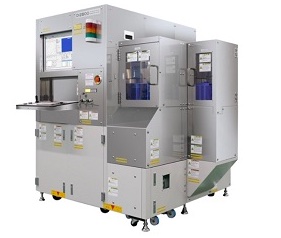
Hitachi High-Tech Corporation announced the launch of the Hitachi Dark Field Wafer Defect Inspection System DI2800, a critical component in any semiconductor manufacturer's metrology capabilities. The DI2800 is a high-speed metrology system designed to identify defects and particles on patterned wafers up to 8 inches (200 mm) in diameter. With its high throughput and performance, the DI2800 can help ensure device reliability and safety, particularly for highly sensitive applications such as Internet of Things (IoT) and automotive fields where 100% inspection is required.
Development Background
With the rise of next generation communication networks (5G) and accelerated adoption of electric vehicles in recent years there has been an increase in demand for semiconductor devices in the IoT and automotive fields where reliability and safety are paramount. In conventional semiconductor device manufacturing, spot-check inspections are performed for the purposes of process management and yield improvement. However, for semiconductor devices used in the IoT and automotive fields, 100% inspection must be carried out to help identify defective products during manufacturing to ensure high reliability and safety. To serve these fields a wafer defect inspection system must have the ability to perform 100% inspection with high sensitivity at high speed.
Key Features
Hitachi High-Tech has developed Dark Field Wafer Defect Inspection System DI2800 to respond to these market needs. This product uses scattering-intensity simulation technology to optimize the illumination and detection optics, enabling highly sensitive inspection of patterned-wafer defects developed during the manufacturing process. It has a detection sensitivity of 0.1-micron standard particle size on mirrored wafers. This performance is even possible on devices as small as 0.3-mm square, which has previously proved challenging due to sensitivity and data processing limitations. With a highly optimized inspection sequence, the DI2800 is capable of throughputs of over 40 200-mm wafers per hour.
Future Initiatives
Hitachi High-Tech will provide this product to customers in combination with the Advanced CD Measurement SEM CS4800 and 3D SEM CT1000, which are already on the market, meeting the diverse metrology needs mass production of semiconductor devices for the IoT and automotive fields. Going forward, Hitachi is committed to product improvement by leveraging data collected from all three product lines to offer new data-based, value-added solutions, contributing to the improved reliability and safety of semiconductor devices in these fields.
Hitachi High-Tech is working to meet customers' needs in metrology and inspection for the R&D and mass production of semiconductor devices by supplying electron beam-based products such as traditional CD-SEM and wafer inspection systems based on optical technologies. Hitachi High-Tech will continue to provide innovative solutions for the upcoming technology challenges. Hitachi High-Tech will contribute to the development of cutting-edge technologies by creating new social and environmental value in collaboration with its customers.


