

















 Elementary, Mr. Watson: Waking Up Europe's PCB Giants
 Connect the Dots: Getting the PCB Quote Right
 Powering the Future: What Engineers Get Wrong About Designing for Reliability





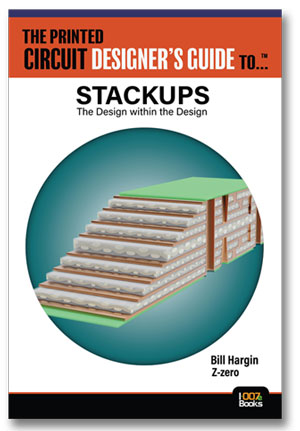
The Printed Circuit Designer’s Guide to... Stackups—The Design within the Design is written by Bill Hargin
Introduction: Mechanical Versus Electrical Worlds
Another book about stackups?
If you’re asking this question, I’d like to know the book you’re thinking of, as I was looking for it a few years back. I have a pretty good PCB signal integrity (SI) library, and I’ve only found one chapter on stackup design so far.
Whenever I talk in person with SI consultants—people who do SI consulting for a living—I ask them, “Of the smoke-jumping projects you’ve been brought in for where there were serious SI problems, how many of those projects have stackup issues?” So far, the only answer I’ve gotten back is, “100 percent.”
The difference between a high-speed PCB design that can be built, and a design that should be built, depends upon the backbone of the design itself: the stackup. The stackup touches every single high-speed signal and yet has had surprisingly little written about it.
In my work, quite a number of PCB stackups cross my desk, and depending on who or what tools were involved in a given design, there are manufacturing parameters that affect both impedance and signal loss that design teams can improve upon.
This book is by no means the last word on the subject, but rather a place to kick off a broader discussion about stackup planning and material selection, to reach the understanding of what I call “the design within the design.”


